TOOLSTICK540DC Silicon Laboratories Inc, TOOLSTICK540DC Datasheet - Page 4
TOOLSTICK540DC
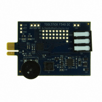
Manufacturer Part Number
TOOLSTICK540DC
Description
DAUGHTER CARD TOOLSTICK F540
Manufacturer
Silicon Laboratories Inc
Series
ToolStickr
Type
MCUr
Datasheets
1.TOOLSTICK540DC.pdf
(274 pages)
2.TOOLSTICK540DC.pdf
(16 pages)
3.TOOLSTICK540DC.pdf
(12 pages)
Specifications of TOOLSTICK540DC
Contents
Daughter Card
Processor To Be Evaluated
C8051F54x
Processor Series
C8051F54x
Interface Type
USB
Operating Supply Voltage
2.7 V to 3.6 V
Lead Free Status / RoHS Status
Lead free / RoHS Compliant
For Use With/related Products
C8051F54x
For Use With
336-1345 - TOOLSTICK BASE ADAPTER336-1182 - ADAPTER USB DEBUG FOR C8051FXXX
Lead Free Status / Rohs Status
Lead free / RoHS Compliant
Other names
336-1717


C8051F54x
15. Power Management Modes................................................................................. 126
16. Reset Sources ...................................................................................................... 129
17. Oscillators and Clock Selection ......................................................................... 135
18. Port Input/Output ................................................................................................. 147
19. Local Interconnect Network (LIN)....................................................................... 170
20. SMBus................................................................................................................... 187
21. UART0 ................................................................................................................... 205
22. Enhanced Serial Peripheral Interface (SPI0) ..................................................... 214
4
15.1. Idle Mode....................................................................................................... 126
15.2. Stop Mode ..................................................................................................... 127
15.3. Suspend Mode .............................................................................................. 127
16.1. Power-On Reset ............................................................................................ 130
16.2. Power-Fail Reset/VDD Monitor ..................................................................... 130
16.3. External Reset ............................................................................................... 132
16.4. Missing Clock Detector Reset ....................................................................... 132
16.5. Comparator0 Reset ....................................................................................... 133
16.6. PCA Watchdog Timer Reset ......................................................................... 133
16.7. Flash Error Reset .......................................................................................... 133
16.8. Software Reset .............................................................................................. 133
17.1. System Clock Selection................................................................................. 135
17.2. Programmable Internal Oscillator .................................................................. 137
17.3. Clock Multiplier .............................................................................................. 140
17.4. External Oscillator Drive Circuit..................................................................... 142
18.1. Port I/O Modes of Operation.......................................................................... 148
18.2. Assigning Port I/O Pins to Analog and Digital Functions............................... 149
18.3. Priority Crossbar Decoder ............................................................................. 150
18.4. Port I/O Initialization ...................................................................................... 152
18.5. Port Match ..................................................................................................... 157
18.6. Special Function Registers for Accessing and Configuring Port I/O ............. 161
19.1. Software Interface with the LIN Controller..................................................... 171
19.2. LIN Interface Setup and Operation................................................................ 171
19.3. LIN Master Mode Operation .......................................................................... 174
19.4. LIN Slave Mode Operation ............................................................................ 175
19.5. Sleep Mode and Wake-Up ............................................................................ 176
19.6. Error Detection and Handling ........................................................................ 176
19.7. LIN Registers................................................................................................. 177
20.1. Supporting Documents .................................................................................. 188
20.2. SMBus Configuration..................................................................................... 188
20.3. SMBus Operation .......................................................................................... 188
20.4. Using the SMBus........................................................................................... 190
20.5. SMBus Transfer Modes................................................................................. 197
20.6. SMBus Status Decoding................................................................................ 201
21.1. Baud Rate Generator .................................................................................... 205
21.2. Data Format................................................................................................... 207
21.3. Configuration and Operation ......................................................................... 208
Rev. 1.1
Related parts for TOOLSTICK540DC
Image
Part Number
Description
Manufacturer
Datasheet
Request
R

Part Number:
Description:
KIT TOOL EVAL SYS IN A USB STICK
Manufacturer:
Silicon Laboratories Inc
Datasheet:

Part Number:
Description:
TOOLSTICK DEBUG ADAPTER
Manufacturer:
Silicon Laboratories Inc
Datasheet:

Part Number:
Description:
TOOLSTICK BASE ADAPTER
Manufacturer:
Silicon Laboratories Inc
Datasheet:

Part Number:
Description:
TOOLSTICK DAUGHTER CARD
Manufacturer:
Silicon Laboratories Inc
Datasheet:

Part Number:
Description:
TOOLSTICK DAUGHTER CARD
Manufacturer:
Silicon Laboratories Inc
Datasheet:

Part Number:
Description:
TOOLSTICK DAUGHTER CARD
Manufacturer:
Silicon Laboratories Inc
Datasheet:

Part Number:
Description:
TOOLSTICK PROGRAMMING ADAPTER
Manufacturer:
Silicon Laboratories Inc
Datasheet:

Part Number:
Description:
TOOLSTICK DAUGHTER CARD
Manufacturer:
Silicon Laboratories Inc
Datasheet:

Part Number:
Description:
KIT STARTER TOOLSTICK
Manufacturer:
Silicon Laboratories Inc
Datasheet:

Part Number:
Description:
KIT UNIVERSITY TOOLSTICK STARTER
Manufacturer:
Silicon Laboratories Inc
Datasheet:

Part Number:
Description:
DAUGHTER CARD TOOLSTICK F330
Manufacturer:
Silicon Laboratories Inc
Datasheet:

Part Number:
Description:
CARD DAUGHTER UNIVRSTY TOOLSTICK
Manufacturer:
Silicon Laboratories Inc
Datasheet:

Part Number:
Description:
DAUGHTER CARD TOOLSTICK F582
Manufacturer:
Silicon Laboratories Inc
Datasheet:

Part Number:
Description:
DAUGHTER CARD TOOLSTICK F500
Manufacturer:
Silicon Laboratories Inc
Datasheet:

Part Number:
Description:
DAUGHTER CARD TOOLSTICK F560
Manufacturer:
Silicon Laboratories Inc
Datasheet: