KIT1925MMA1250D Freescale Semiconductor, KIT1925MMA1250D Datasheet - Page 3
KIT1925MMA1250D
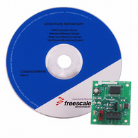
Manufacturer Part Number
KIT1925MMA1250D
Description
KIT SENSOR ACCEL MMA1250D
Manufacturer
Freescale Semiconductor
Datasheet
1.KIT1925MMA1250D.pdf
(9 pages)
Specifications of KIT1925MMA1250D
Mfg Application Notes
Using an Accelerometer Eval Board, AppNote
Lead Free Status / RoHS Status
Contains lead / RoHS non-compliant


Sensors
Freescale Semiconductor
Table 2. Operating Characteristics
(Unless otherwise noted: –40°C ≤ T
10. The Status pin output latches high if a Low Voltage Detection or Clock Frequency failure occurs, or the EPROM parity changes to odd. The
11. Time for amplifiers to recover after an acceleration signal causes them to saturate.
12. Preserves phase margin (60°) to guarantee output amplifier stability.
13. A measure of the device's ability to reject an acceleration applied 90° from the true axis of sensitivity.
Operating Range
Output Signal
Noise
Self-Test
Status
Output Stage Performance
Mechanical Characteristics
1. For a loaded output the measurements are observed after an RC filter consisting of a 1 kΩ resistor and a 0.1 μF capacitor to ground.
2. These limits define the range of operation for which the part will meet specification.
3. Within the supply range of 4.75 and 5.25 volts, the device operates as a fully calibrated linear accelerometer. Beyond these supply limits the
4. The device can measure both + and – acceleration. With no input acceleration the output is at midsupply. For positive acceleration the output
5. The device is calibrated at 3g. Sensitivity limits apply to 0Hz acceleration.
6. At clock frequency ≅70 kHz.
7. The digital input pin has an internal pull-down current source to prevent inadvertent self test initiation due to external board level leakages.
8. Time for the output to reach 90% of its final value after a self-test is initiated.
9. The Status pin output is not valid following power-up until at least one rising edge has been applied to the self-test pin. The Status pin is high
Supply Voltage
Supply Current
Operating Temperature Range
Acceleration Range
Zero g (T
Zero g (V
Sensitivity (T
Sensitivity (V
Bandwidth Response
Nonlinearity
RMS (0.1 Hz – 1.0 kHz)
Spectral Density (RMS, 0.1 Hz – 1.0 KHz)
Output Response (V
Input Low
Input High
Input Loading
Response Time
Output Low (I
Output High (I
Electrical Saturation Recovery Time
Full Scale Output Range (I
Capacitive Load Drive
Output Impedance
Transverse Sensitivity
device may operate as a linear device but is not guaranteed to be in calibration.
will increase above V
whenever the self-test input is high, as a means to check the connectivity of the self-test and Status pins in the application.
Status pin can be reset low if the self-test pin is pulsed with a high input for at least 100 μs, unless a fault condition continues to exist.
(9), (10)
A
DD
= 25°C, V
= 5.0 V)
A
DD
load
(7)
load
(2)
= 25°C, V
(3)
(8)
= 5.0 V)
= 100 μA)
= 100 μA)
DD
DD
Characteristic
DD
(12)
(13)
= 5.0 V)
= 5.0 V)
/2 and for negative acceleration the output will decrease below V
DD
OUT
= 5.0 V)
= 200 μA)
(4)
(5)
(11)
A
≤ +105°C, 4.75 ≤ V
(6)
DD
≤ 5.25, Acceleration = 0g, Loaded output.
Symbol
NL
t
V
V
V
n
ΔV
DELAY
V
f
V
V
g
n
V
XZ,YZ
I
V
-3dB
V
t
T
RMS
C
Z
I
FSO
DD
OFF
OFF
S
S
ST
SD
IN
OH
DD
FS
OUT
OL
IH
A
IL
O
ST
L
V
V
0.7 V
SS
DD
–300
4.75
2.25
42.5
–1.0
Min
V
–40
380
370
1.1
2.0
1.0
—
—
—
—
—
—
—
—
—
+ 0.25
SS
– 0.8
DD
DD
/2.
–125
5.00
1.25
Typ
400
400
700
2.1
2.5
2.5
2.0
2.0
50
50
—
—
—
—
—
—
—
—
—
—
5
(1)
V
DD
0.3 V
)
430.1
+105
+1.0
Max
5.25
2.75
57.5
V
420
–50
100
3.0
3.0
4.0
1.5
0.4
2.0
5.0
25
—
—
—
—
– 0.25
DD
DD
MMA1250KEG
μg/
% FSO
% FSO
mVrms
mV/g
mV/g
Unit
mA
ms
ms
Hz
μA
°C
pF
Ω
V
g
V
V
V
V
V
V
V
V
Hz
3
Related parts for KIT1925MMA1250D
Image
Part Number
Description
Manufacturer
Datasheet
Request
R

Part Number:
Description:
Manufacturer:
Freescale Semiconductor, Inc
Datasheet:
Part Number:
Description:
Manufacturer:
Freescale Semiconductor, Inc
Datasheet:
Part Number:
Description:
Manufacturer:
Freescale Semiconductor, Inc
Datasheet:
Part Number:
Description:
Manufacturer:
Freescale Semiconductor, Inc
Datasheet:
Part Number:
Description:
Manufacturer:
Freescale Semiconductor, Inc
Datasheet:
Part Number:
Description:
Manufacturer:
Freescale Semiconductor, Inc
Datasheet:
Part Number:
Description:
Manufacturer:
Freescale Semiconductor, Inc
Datasheet:
Part Number:
Description:
Manufacturer:
Freescale Semiconductor, Inc
Datasheet:
Part Number:
Description:
Manufacturer:
Freescale Semiconductor, Inc
Datasheet:
Part Number:
Description:
Manufacturer:
Freescale Semiconductor, Inc
Datasheet:
Part Number:
Description:
Manufacturer:
Freescale Semiconductor, Inc
Datasheet:
Part Number:
Description:
Manufacturer:
Freescale Semiconductor, Inc
Datasheet:
Part Number:
Description:
Manufacturer:
Freescale Semiconductor, Inc
Datasheet:
Part Number:
Description:
Manufacturer:
Freescale Semiconductor, Inc
Datasheet:
Part Number:
Description:
Manufacturer:
Freescale Semiconductor, Inc
Datasheet: