PESD3V3S2UQ,115 NXP Semiconductors, PESD3V3S2UQ,115 Datasheet
PESD3V3S2UQ,115
Specifications of PESD3V3S2UQ,115
934057839115
PESD3V3S2UQ T/R
PESD3V3S2UQ T/R


Related parts for PESD3V3S2UQ,115


PESD3V3S2UQ,115 Summary of contents
Page 1
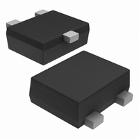
PESDxS2UQ series Double ESD protection diodes in SOT663 package Rev. 04 — 26 January 2010 1. Product profile 1.1 General description Unidirectional double ElectroStatic Discharge (ESD) protection diodes in a SOT663 ultra small and flat lead Surface-Mounted Device (SMD) plastic ...
Page 2
... NXP Semiconductors 2. Pinning information Table 2. Pin Ordering information Table 3. Type number PESD3V3S2UQ PESD5V0S2UQ PESD12VS2UQ PESD15VS2UQ PESD24VS2UQ 4. Marking Table 4. Type number PESD3V3S2UQ PESD5V0S2UQ PESD12VS2UQ PESD15VS2UQ PESD24VS2UQ PESDXS2UQ_SER_4 Product data sheet Double ESD protection diodes in SOT663 package Pinning Description cathode 1 cathode 2 common anode ...
Page 3
... NXP Semiconductors 5. Limiting values Table 5. In accordance with the Absolute Maximum Rating System (IEC 60134). Symbol Per diode Per device amb T stg Non-repetitive current pulse 8/20 μs exponential decay waveform according to IEC 61000-4-5. [1] [2] Measured across either pins 1 and 3 or pins 2 and 3. ...
Page 4
... NXP Semiconductors 120 ; 8 μs 100 % (%) 80 − 8/20 μs pulse waveform according to Fig 1. IEC 61000-4-5 6. Characteristics Table 8. ° Symbol Per diode V RWM PESDXS2UQ_SER_4 Product data sheet Double ESD protection diodes in SOT663 package 001aaa630 ; 20 μ (μs) Fig 2. Characteristics C unless otherwise specified. Parameter Conditions ...
Page 5
... NXP Semiconductors Table 8. ° Symbol dif Non-repetitive current pulse 8/20 μs exponential decay waveform according to IEC 61000-4-5. [1] [2] Measured across either pins 1 and 3 or pins 2 and 3. PESDXS2UQ_SER_4 Product data sheet Double ESD protection diodes in SOT663 package Characteristics …continued C unless otherwise specified. ...
Page 6
... NXP Semiconductors ( °C T amb Fig 3. Peak pulse power dissipation as a function of pulse duration; typical values 240 C d (pF) 200 160 (1) 120 ( ° MHz; T amb (1) PESD3V3S2UQ 3.3 V RWM (2) PESD5V0S2UQ RWM Fig 5. Diode capacitance as a function of reverse voltage; typical values PESDXS2UQ_SER_4 Product data sheet ...
Page 7
... NXP Semiconductors (1) PESD3V3S2UQ 3.3 V RWM (2) PESD5V0S2UQ RWM is less than 150 °C for PESD12VS2UQ RWM PESD15VS2UQ RWM PESD24VS2UQ RWM Fig 7. Relative variation of reverse leakage current as a function of junction temperature; typical values PESDXS2UQ_SER_4 Product data sheet Double ESD protection diodes in SOT663 package RM(25°C) 1 − ...
Page 8
... NXP Semiconductors ESD TESTER note 1 Note 1: IEC61000-4-2 network = 330 Ω 150 pF vertical scale = 200 V/div horizontal scale = 50 ns/div GND unclamped +1 kV ESD voltage waveform (IEC61000-4-2 network) GND vertical scale = 200 V/div horizontal scale = 50 ns/div unclamped −1 kV ESD voltage waveform (IEC61000-4-2 network) Fig 8 ...
Page 9
... NXP Semiconductors 7. Application information The PESDxS2UQ series is designed for the protection two unidirectional data lines from the damage caused by ESD and surge pulses. The devices may be used on lines where the signal polarities are below ground. The PESDxS2UQ series provides a surge capability 150 W (P Fig 9 ...
Page 10
... NXP Semiconductors 8. Package outline Fig 10. Package outline PESDxS2UQ series (SOT663) 9. Packing information Table 9. The indicated -xxx are the last three digits of the 12NC ordering code. Type number PESD3V3S2UQ PESD5V0S2UQ PESD12VS2UQ PESD15VS2UQ PESD24VS2UQ PESD3V3S2UQ PESD5V0S2UQ PESD12VS2UQ PESD15VS2UQ PESD24VS2UQ [1] For further information and the availability of packing methods, see ...
Page 11
... Release date PESDXS2UQ_SER_4 20100126 • Modifications: The format of this data sheet has been redesigned to comply with the new identity guidelines of NXP Semiconductors. • Legal texts have been adapted to the new company name where appropriate. • Section 1.1 “General • Section 1.4 “Quick reference • ...
Page 12
... Right to make changes — NXP Semiconductors reserves the right to make changes to information published in this document, including without limitation specifications and product descriptions, at any time and without notice ...
Page 13
... NXP Semiconductors 13. Contents 1 Product profile . . . . . . . . . . . . . . . . . . . . . . . . . . 1 1.1 General description . . . . . . . . . . . . . . . . . . . . . 1 1.2 Features . . . . . . . . . . . . . . . . . . . . . . . . . . . . . . 1 1.3 Applications . . . . . . . . . . . . . . . . . . . . . . . . . . . 1 1.4 Quick reference data . . . . . . . . . . . . . . . . . . . . 1 2 Pinning information . . . . . . . . . . . . . . . . . . . . . . 2 3 Ordering information . . . . . . . . . . . . . . . . . . . . . 2 4 Marking . . . . . . . . . . . . . . . . . . . . . . . . . . . . . . . . 2 5 Limiting values Characteristics . . . . . . . . . . . . . . . . . . . . . . . . . . 4 7 Application information Package outline . . . . . . . . . . . . . . . . . . . . . . . . 10 9 Packing information . . . . . . . . . . . . . . . . . . . . 10 10 Revision history . . . . . . . . . . . . . . . . . . . . . . . . 11 11 Legal information ...