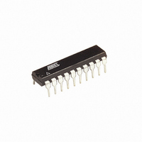
ATTINY2313V-10PU Atmel, ATTINY2313V-10PU Datasheet - Page 169

ATTINY2313V-10PU
Manufacturer Part Number
ATTINY2313V-10PU
Description
IC MCU AVR 2K FLASH 20DIP
Manufacturer
Atmel
Series
AVR® ATtinyr
Datasheets
1.ATTINY2313-20MU.pdf
(226 pages)
2.ATTINY2313V-10MU.pdf
(15 pages)
3.ATTINY2313V-10SU.pdf
(20 pages)
Specifications of ATTINY2313V-10PU
Core Processor
AVR
Core Size
8-Bit
Speed
10MHz
Connectivity
SPI, UART/USART
Peripherals
Brown-out Detect/Reset, POR, PWM, WDT
Number Of I /o
18
Program Memory Size
2KB (1K x 16)
Program Memory Type
FLASH
Eeprom Size
128 x 8
Ram Size
128 x 8
Voltage - Supply (vcc/vdd)
1.8 V ~ 5.5 V
Oscillator Type
Internal
Operating Temperature
-40°C ~ 85°C
Package / Case
20-DIP (0.300", 7.62mm)
Processor Series
ATTINY2x
Core
AVR8
Data Bus Width
8 bit
Data Ram Size
128 B
Interface Type
SPI/UART/USI
Maximum Clock Frequency
10 MHz
Number Of Programmable I/os
18
Number Of Timers
2
Operating Supply Voltage
1.8 V to 5.5 V
Maximum Operating Temperature
+ 85 C
Mounting Style
Through Hole
Minimum Operating Temperature
- 40 C
Package
20PDIP
Device Core
AVR
Family Name
ATtiny
Maximum Speed
10 MHz
Data Rom Size
128 B
Height
4.95 mm
Length
26.92 mm
Supply Voltage (max)
5.5 V
Supply Voltage (min)
1.8 V
Width
7.11 mm
For Use With
ATSTK600-DIP40 - STK600 SOCKET/ADAPTER 40-PDIP770-1007 - ISP 4PORT ATMEL AVR MCU SPI/JTAGATAVRDRAGON - KIT DRAGON 32KB FLASH MEM AVRATAVRISP2 - PROGRAMMER AVR IN SYSTEMATJTAGICE2 - AVR ON-CHIP D-BUG SYSTEM
Lead Free Status / RoHS Status
Lead free / RoHS Compliant
Data Converters
-
Lead Free Status / Rohs Status
Lead free / RoHS Compliant
Available stocks
Company
Part Number
Manufacturer
Quantity
Price
Company:
Part Number:
ATTINY2313V-10PU
Manufacturer:
ATMEL
Quantity:
3 000
Part Number:
ATTINY2313V-10PU
Manufacturer:
ATMEL/爱特梅尔
Quantity:
20 000
Programming the
Lock Bits
Reading the Fuse and
Lock Bits
Reading the Signature
Bytes
2543L–AVR–08/10
The algorithm for programming the Lock bits is as follows (refer to
page 165
1. A: Load Command “0010 0000”.
2. C: Load Data Low Byte. Bit n = “0” programs the Lock bit. If LB mode 3 is programmed
3. Give WR a negative pulse and wait for RDY/BSY to go high.
The Lock bits can only be cleared by executing Chip Erase.
The algorithm for reading the Fuse and Lock bits is as follows (refer to
on page 165
1. A: Load Command “0000 0100”.
2. Set OE to “0”, BS2 to “0” and BS1 to “0”. The status of the Fuse Low bits can now be
3. Set OE to “0”, BS2 to “1” and BS1 to “1”. The status of the Fuse High bits can now be
4. Set OE to “0”, BS2 to “1”, and BS1 to “0”. The status of the Extended Fuse bits can now
5. Set OE to “0”, BS2 to “0” and BS1 to “1”. The status of the Lock bits can now be read at
6. Set OE to “1”.
Figure 74. Mapping Between BS1, BS2 and the Fuse and Lock Bits During Read
The algorithm for reading the Signature bytes is as follows (refer to
page 165
1. A: Load Command “0000 1000”.
2. B: Load Address Low Byte (0x00 - 0x02).
3. Set OE to “0”, and BS to “0”. The selected Signature byte can now be read at DATA.
4. Set OE to “1”.
(LB1 and LB2 is programmed), it is not possible to program the Boot Lock bits by any
External Programming mode.
read at DATA (“0” means programmed).
read at DATA (“0” means programmed).
be read at DATA (“0” means programmed).
DATA (“0” means programmed).
for details on Command and Data loading):
for details on Command and Address loading):
for details on Command loading):
Extended Fuse Byte
Fuse Low Byte
Fuse High Byte
Lock Bits
BS2
BS2
0
1
0
1
BS1
0
1
“Programming the Flash” on
“Programming the Flash” on
“Programming the Flash”
DATA
169


