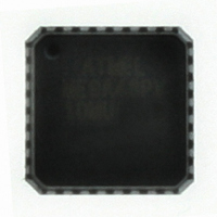
ATMEGA48PV-10MU Atmel, ATMEGA48PV-10MU Datasheet - Page 302

ATMEGA48PV-10MU
Manufacturer Part Number
ATMEGA48PV-10MU
Description
MCU AVR 4K ISP FLASH 10MHZ 32QFN
Manufacturer
Atmel
Series
AVR® ATmegar
Specifications of ATMEGA48PV-10MU
Core Processor
AVR
Core Size
8-Bit
Speed
10MHz
Connectivity
I²C, SPI, UART/USART
Peripherals
Brown-out Detect/Reset, POR, PWM, WDT
Number Of I /o
23
Program Memory Size
4KB (2K x 16)
Program Memory Type
FLASH
Eeprom Size
256 x 8
Ram Size
512 x 8
Voltage - Supply (vcc/vdd)
1.8 V ~ 5.5 V
Data Converters
A/D 8x10b
Oscillator Type
Internal
Operating Temperature
-40°C ~ 85°C
Package / Case
32-VQFN Exposed Pad, 32-HVQFN, 32-SQFN, 32-DHVQFN
Processor Series
ATMEGA48x
Core
AVR8
Data Bus Width
8 bit
Data Ram Size
512 B
Interface Type
I2C, SPI, USART
Maximum Clock Frequency
10 MHz
Number Of Programmable I/os
23
Number Of Timers
3
Maximum Operating Temperature
+ 85 C
Mounting Style
SMD/SMT
Minimum Operating Temperature
- 40 C
On-chip Adc
10 bit, 8 Channel
For Use With
ATSTK600-TQFP32 - STK600 SOCKET/ADAPTER 32-TQFPATSTK600 - DEV KIT FOR AVR/AVR32770-1007 - ISP 4PORT ATMEL AVR MCU SPI/JTAGATAVRDRAGON - KIT DRAGON 32KB FLASH MEM AVRATAVRISP2 - PROGRAMMER AVR IN SYSTEMATJTAGICE2 - AVR ON-CHIP D-BUG SYSTEM
Lead Free Status / RoHS Status
Lead free / RoHS Compliant
Available stocks
Company
Part Number
Manufacturer
Quantity
Price
Part Number:
ATMEGA48PV-10MU
Manufacturer:
ATMEL/爱特梅尔
Quantity:
20 000
- Current page: 302 of 420
- Download datasheet (9Mb)
27.7.8
27.7.9
27.7.10
27.7.11
8025L–AVR–7/10
Programming the Fuse Low Bits
Programming the Fuse High Bits
Programming the Extended Fuse Bits
Programming the Lock Bits
The algorithm for programming the Fuse Low bits is as follows (refer to
on page 298
1. A: Load Command “0100 0000”.
2. C: Load Data Low Byte. Bit n = “0” programs and bit n = “1” erases the Fuse bit.
3. Give WR a negative pulse and wait for RDY/BSY to go high.
The algorithm for programming the Fuse High bits is as follows (refer to
Flash” on page 298
1. A: Load Command “0100 0000”.
2. C: Load Data Low Byte. Bit n = “0” programs and bit n = “1” erases the Fuse bit.
3. Set BS1 to “1” and BS2 to “0”. This selects high data byte.
4. Give WR a negative pulse and wait for RDY/BSY to go high.
5. Set BS1 to “0”. This selects low data byte.
The algorithm for programming the Extended Fuse bits is as follows (refer to
Flash” on page 298
1. 1. A: Load Command “0100 0000”.
2. 2. C: Load Data Low Byte. Bit n = “0” programs and bit n = “1” erases the Fuse bit.
3. 3. Set BS1 to “0” and BS2 to “1”. This selects extended data byte.
4. 4. Give WR a negative pulse and wait for RDY/BSY to go high.
5. 5. Set BS2 to “0”. This selects low data byte.
Figure 27-5. Programming the FUSES Waveforms
The algorithm for programming the Lock bits is as follows (refer to
page 298
RESET +12V
RDY/BSY
PAGEL
XTAL1
DATA
for details on Command and Data loading):
XA1
XA0
BS1
BS2
WR
OE
for details on Command and Data loading):
0x40
A
for details on Command and Data loading):
for details on Command and Data loading):
DATA
C
Write Fuse Low byte
XX
0x40
A
DATA
C
Write Fuse high byte
XX
ATmega48P/88P/168P
”Programming the Flash” on
0x40
A
”Programming the Flash”
DATA
C
Write Extended Fuse byte
”Programming the
”Programming the
XX
302
Related parts for ATMEGA48PV-10MU
Image
Part Number
Description
Manufacturer
Datasheet
Request
R

Part Number:
Description:
Manufacturer:
Atmel Corporation
Datasheet:

Part Number:
Description:
MCU AVR 4K ISP FLASH 20MHZ 32QFN
Manufacturer:
Atmel
Datasheet:

Part Number:
Description:
MCU AVR 4K ISP FLSH 20MHZ 32TQFP
Manufacturer:
Atmel
Datasheet:

Part Number:
Description:
MCU AVR 4K ISP FLASH 20MHZ 28DIP
Manufacturer:
Atmel
Datasheet:

Part Number:
Description:
MCU AVR 4K FLASH 20MHZ 32TQFP
Manufacturer:
Atmel
Datasheet:

Part Number:
Description:
MCU AVR 4K FLASH 20MHZ 32QFN
Manufacturer:
Atmel
Datasheet:

Part Number:
Description:
MCU AVR 4K FLASH 20MHZ 28-QFN
Manufacturer:
Atmel
Datasheet:

Part Number:
Description:
MCU AVR 4K FLASH 20MHZ 28QFN
Manufacturer:
Atmel
Datasheet:

Part Number:
Description:
IC AVR MCU 4K 5V 20MHZ 32-TQFP
Manufacturer:
Atmel
Datasheet:

Part Number:
Description:
Manufacturer:
Atmel Corporation
Datasheet:

Part Number:
Description:
Manufacturer:
Atmel Corporation
Datasheet:


