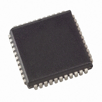
ATMEGA8535L-8JU Atmel, ATMEGA8535L-8JU Datasheet - Page 144

ATMEGA8535L-8JU
Manufacturer Part Number
ATMEGA8535L-8JU
Description
MCU AVR 8K ISP FLASH MEM 44-PLCC
Manufacturer
Atmel
Series
AVR® ATmegar
Specifications of ATMEGA8535L-8JU
Core Processor
AVR
Core Size
8-Bit
Speed
8MHz
Connectivity
I²C, SPI, UART/USART
Peripherals
Brown-out Detect/Reset, POR, PWM, WDT
Number Of I /o
32
Program Memory Size
8KB (4K x 16)
Program Memory Type
FLASH
Eeprom Size
512 x 8
Ram Size
512 x 8
Voltage - Supply (vcc/vdd)
2.7 V ~ 5.5 V
Data Converters
A/D 8x10b
Oscillator Type
Internal
Operating Temperature
-40°C ~ 85°C
Package / Case
44-PLCC
Processor Series
ATMEGA8x
Core
AVR8
Data Bus Width
8 bit
Data Ram Size
512 B
Interface Type
2-Wire, SPI, USART
Maximum Clock Frequency
8 MHz
Number Of Programmable I/os
32
Number Of Timers
3
Maximum Operating Temperature
+ 85 C
Mounting Style
SMD/SMT
3rd Party Development Tools
EWAVR, EWAVR-BL
Minimum Operating Temperature
- 40 C
On-chip Adc
10 bit, 8 Channel
Cpu Family
ATmega
Device Core
AVR
Device Core Size
8b
Frequency (max)
8MHz
Total Internal Ram Size
512Byte
# I/os (max)
32
Number Of Timers - General Purpose
3
Operating Supply Voltage (typ)
3.3/5V
Operating Supply Voltage (max)
5.5V
Operating Supply Voltage (min)
2.7V
Instruction Set Architecture
RISC
Operating Temp Range
-40C to 85C
Operating Temperature Classification
Industrial
Mounting
Surface Mount
Pin Count
44
Package Type
PLCC
For Use With
ATSTK600 - DEV KIT FOR AVR/AVR32770-1007 - ISP 4PORT ATMEL AVR MCU SPI/JTAGATAVRISP2 - PROGRAMMER AVR IN SYSTEMATSTK500 - PROGRAMMER AVR STARTER KIT
Lead Free Status / RoHS Status
Lead free / RoHS Compliant
Available stocks
Company
Part Number
Manufacturer
Quantity
Price
- Current page: 144 of 321
- Download datasheet (3Mb)
Data Modes
144
ATmega8535(L)
There are four combinations of SCK phase and polarity with respect to serial data,
which are determined by control bits CPHA and CPOL. The SPI data transfer formats
are shown in Figure 67 and Figure 68. Data bits are shifted out and latched in on oppo-
site edges of the SCK signal, ensuring sufficient time for data signals to stabilize. This is
clearly seen by summarizing Table 57 and Table 58, as done below:
Table 60. CPOL Functionality
Figure 67. SPI Transfer Format with CPHA = 0
Figure 68. SPI Transfer Format with CPHA = 1
SCK (CPOL = 0)
mode 0
SCK (CPOL = 1)
mode 2
SAMPLE I
MOSI/MISO
CHANGE 0
MOSI PIN
CHANGE 0
MISO PIN
SCK (CPOL = 0)
mode 1
SCK (CPOL = 1)
mode 3
SAMPLE I
MOSI/MISO
CHANGE 0
MOSI PIN
CHANGE 0
MISO PIN
SS
SS
CPOL=0, CPHA=0
CPOL=0, CPHA=1
CPOL=1, CPHA=0
CPOL=1, CPHA=1
MSB first (DORD = 0)
LSB first (DORD = 1)
MSB first (DORD = 0)
LSB first (DORD = 1)
MSB
LSB
MSB
LSB
Bit 6
Bit 1
Sample (Falling)
Sample (Rising)
Leading Edge
Setup (Falling)
Setup (Rising)
Bit 6
Bit 1
Bit 5
Bit 2
Bit 5
Bit 2
Bit 4
Bit 3
Bit 4
Bit 3
Sample (Falling)
Sample (Rising)
Bit 3
Bit 4
Setup (Falling)
Setup (Rising)
Trailing Edge
Bit 3
Bit 4
Bit 2
Bit 5
Bit 2
Bit 5
Bit 1
Bit 6
Bit 1
Bit 6
2502K–AVR–10/06
SPI Mode
LSB
MSB
0
1
2
3
LSB
MSB
Related parts for ATMEGA8535L-8JU
Image
Part Number
Description
Manufacturer
Datasheet
Request
R

Part Number:
Description:
IC AVR MCU 2.4GHZ XCEIVER 64QFN
Manufacturer:
Atmel
Datasheet:

Part Number:
Description:
Manufacturer:
Atmel
Datasheet:

Part Number:
Description:
MCU ATMEGA644/AT86RF230 40-DIP
Manufacturer:
Atmel
Datasheet:

Part Number:
Description:
BUNDLE ATMEGA644P/AT86RF230 QFN
Manufacturer:
Atmel
Datasheet:

Part Number:
Description:
BUNDLE ATMEGA644P/AT86RF230 TQFP
Manufacturer:
Atmel
Datasheet:

Part Number:
Description:
MCU ATMEGA1281/AT86RF230 64-TQFP
Manufacturer:
Atmel
Datasheet:

Part Number:
Description:
MCU ATMEGA1280/AT86RF230 100TQFP
Manufacturer:
Atmel
Datasheet:

Part Number:
Description:
BUNDLE ATMEGA1280/AT86RF100-TQFP
Manufacturer:
Atmel
Datasheet:

Part Number:
Description:
BUNDLE ATMEGA2560V/AT86RF230-ZU
Manufacturer:
Atmel
Datasheet:

Part Number:
Description:
MCU ATMEGA2561/AT86RF230 64-TQFP
Manufacturer:
Atmel
Datasheet:

Part Number:
Description:
INTERVAL AND WIPE/WASH WIPER CONTROL IC WITH DELAY
Manufacturer:
ATMEL Corporation
Datasheet:

Part Number:
Description:
Low-Voltage Voice-Switched IC for Hands-Free Operation
Manufacturer:
ATMEL Corporation
Datasheet:

Part Number:
Description:
MONOLITHIC INTEGRATED FEATUREPHONE CIRCUIT
Manufacturer:
ATMEL Corporation
Datasheet:

Part Number:
Description:
AM-FM Receiver IC U4255BM-M
Manufacturer:
ATMEL Corporation
Datasheet:


