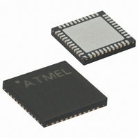
ATMEGA164P-20MU Atmel, ATMEGA164P-20MU Datasheet - Page 261

ATMEGA164P-20MU
Manufacturer Part Number
ATMEGA164P-20MU
Description
IC MCU AVR 16K FLASH 44-QFN
Manufacturer
Atmel
Series
AVR® ATmegar
Specifications of ATMEGA164P-20MU
Core Processor
AVR
Core Size
8-Bit
Speed
20MHz
Connectivity
I²C, SPI, UART/USART
Peripherals
Brown-out Detect/Reset, POR, PWM, WDT
Number Of I /o
32
Program Memory Size
16KB (8K x 16)
Program Memory Type
FLASH
Eeprom Size
512 x 8
Ram Size
1K x 8
Voltage - Supply (vcc/vdd)
2.7 V ~ 5.5 V
Data Converters
A/D 8x10b
Oscillator Type
Internal
Operating Temperature
-40°C ~ 85°C
Package / Case
44-VQFN Exposed Pad
Processor Series
ATMEGA16x
Core
AVR8
Data Bus Width
8 bit
Data Ram Size
1 KB
Interface Type
2-Wire/JTAG/SPI/USART
Maximum Clock Frequency
20 MHz
Number Of Programmable I/os
32
Number Of Timers
3
Maximum Operating Temperature
+ 85 C
Mounting Style
SMD/SMT
3rd Party Development Tools
EWAVR, EWAVR-BL
Development Tools By Supplier
ATAVRDRAGON, ATSTK500, ATSTK600, ATAVRISP2, ATAVRONEKIT
Minimum Operating Temperature
- 40 C
On-chip Adc
8-ch x 10-bit
Package
44MLF
Device Core
AVR
Family Name
ATmega
Maximum Speed
20 MHz
Operating Supply Voltage
3.3|5 V
For Use With
ATSTK600-TQFP44 - STK600 SOCKET/ADAPTER 44-TQFPATSTK600 - DEV KIT FOR AVR/AVR32770-1007 - ISP 4PORT ATMEL AVR MCU SPI/JTAGATAVRISP2 - PROGRAMMER AVR IN SYSTEM
Lead Free Status / RoHS Status
Lead free / RoHS Compliant
Available stocks
Company
Part Number
Manufacturer
Quantity
Price
Part Number:
ATMEGA164P-20MU
Manufacturer:
ATMEL/爱特梅尔
Quantity:
20 000
- Current page: 261 of 439
- Download datasheet (10Mb)
Figure 21-1. Block Diagram
8011O–AVR–07/10
TDI
TDO
TCK
TMS
CONTROLLER
M
U
X
TAP
DEVICE BOUNDARY
INSTRUCTION
BREAKPOINT
SCAN CHAIN
REGISTER
REGISTER
REGISTER
BYPASS
ID
• TCK: Test Clock. JTAG operation is synchronous to TCK.
• TDI: Test Data In. Serial input data to be shifted in to the Instruction Register or Data Register
• TDO: Test Data Out. Serial output data from Instruction Register or Data Register.
The IEEE std. 1149.1 also specifies an optional TAP signal; TRST – Test ReSeT – which is not
provided.
When the JTAGEN Fuse is unprogrammed, these four TAP pins are normal port pins, and the
TAP controller is in reset. When programmed, the input TAP signals are internally pulled high
and the JTAG is enabled for Boundary-scan and programming. The device is shipped with this
fuse programmed.
For the On-chip Debug system, in addition to the JTAG interface pins, the RESET pin is moni-
tored by the debugger to be able to detect external reset sources. The debugger can also pull
the RESET pin low to reset the whole system, assuming only open collectors on the reset line
are used in the application.
(Scan Chains).
DECODER
ADDRESS
JTAG PROGRAMMING
MEMORY
FLASH
AND CONTROL
BREAKPOINT
OCD STATUS
INTERFACE
UNIT
Address
Data
I/O PORT 0
I/O PORT n
INTERNAL
FLOW CONTROL
CHAIN
SCAN
UNIT
BOUNDARY SCAN CHAIN
PC
Instruction
JTAG / AVR CORE
COMMUNICATION
PERIPHERAL
INTERFACE
AVR CPU
DIGITAL
UNITS
ATmega164P/324P/644P
PERIPHERIAL
ANALOG
UNITS
Control & Clock lines
Analog inputs
261
Related parts for ATMEGA164P-20MU
Image
Part Number
Description
Manufacturer
Datasheet
Request
R

Part Number:
Description:
8-bit Microcontroller With 16/32/64k Bytes In-system Programmable Flash - Atmel Corporation
Manufacturer:
ATMEL Corporation
Datasheet:

Part Number:
Description:
8-bit Microcontroller with 16/32/64K Bytes In-System Programmable Flash
Manufacturer:
ATMEL [ATMEL Corporation]
Datasheet:

Part Number:
Description:
Manufacturer:
Atmel Corporation
Datasheet:

Part Number:
Description:
IC AVR MCU 16K 16MHZ 5V 44TQFP
Manufacturer:
Atmel
Datasheet:

Part Number:
Description:
IC AVR MCU 16K 16MHZ 5V 44-QFN
Manufacturer:
Atmel
Datasheet:

Part Number:
Description:
IC AVR MCU 16K 16MHZ 5V 40DIP
Manufacturer:
Atmel
Datasheet:

Part Number:
Description:
MCU AVR 16K FLASH 16MHZ 44-QFN
Manufacturer:
Atmel
Datasheet:

Part Number:
Description:
IC AVR MCU 16K 16MHZ COM 40-DIP
Manufacturer:
Atmel
Datasheet:

Part Number:
Description:
IC AVR MCU 16K 16MHZ COM 44-QFN
Manufacturer:
Atmel
Datasheet:

Part Number:
Description:
IC AVR MCU 16K 16MHZ IND 40-DIP
Manufacturer:
Atmel
Datasheet:

Part Number:
Description:
IC AVR MCU 16K 16MHZ IND 44-QFN
Manufacturer:
Atmel
Datasheet:

Part Number:
Description:
IC AVR MCU 16K 16MHZ IND 44-TQFP
Manufacturer:
Atmel
Datasheet:

Part Number:
Description:
IC MCU 8BIT 16KB FLASH 44TQFP
Manufacturer:
Atmel
Datasheet:

Part Number:
Description:
MCU AVR 16K FLASH 16MHZ 44-TQFP
Manufacturer:
Atmel
Datasheet:


