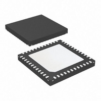
AT91SAM7S32B-MU Atmel, AT91SAM7S32B-MU Datasheet - Page 152

AT91SAM7S32B-MU
Manufacturer Part Number
AT91SAM7S32B-MU
Description
IC MCU ARM7 32KB FLASH 48-VQFN
Manufacturer
Atmel
Series
AT91SAMr
Datasheet
1.AT91SAM7S16-MU.pdf
(779 pages)
Specifications of AT91SAM7S32B-MU
Core Processor
ARM7
Core Size
16/32-Bit
Speed
55MHz
Connectivity
I²C, SPI, SSC, UART/USART
Peripherals
Brown-out Detect/Reset, DMA, POR, PWM, WDT
Number Of I /o
21
Program Memory Size
32KB (32K x 8)
Program Memory Type
FLASH
Ram Size
8K x 8
Voltage - Supply (vcc/vdd)
1.65 V ~ 1.95 V
Data Converters
A/D 8x10b
Oscillator Type
Internal
Operating Temperature
-40°C ~ 85°C
Package / Case
48-VQFN Exposed Pad, 48-HVQFN, 48-SQFN, 48-DHVQFN
For Use With
AT91SAM-ICE - EMULATOR FOR AT91 ARM7/ARM9AT91SAM7S-EK - KIT EVAL FOR ARM AT91SAM7S
Lead Free Status / RoHS Status
Lead free / RoHS Compliant
Eeprom Size
-
Available stocks
Company
Part Number
Manufacturer
Quantity
Price
- Current page: 152 of 779
- Download datasheet (11Mb)
22.3
22.3.1
22.3.2
22.3.3
152
Functional Description
AT91SAM7S Series Preliminary
Configuration
Memory Pointers
Transfer Counters
The PDC channels user interface enables the user to configure and control the data transfers for
each channel. The user interface of a PDC channel is integrated into the user interface of the
peripheral (offset 0x100), which it is related to.
Per peripheral, it contains four 32-bit Pointer Registers (RPR, RNPR, TPR, and TNPR) and four
16-bit Counter Registers (RCR, RNCR, TCR, and TNCR).
The size of the buffer (number of transfers) is configured in an internal 16-bit transfer counter
register, and it is possible, at any moment, to read the number of transfers left for each channel.
The memory base address is configured in a 32-bit memory pointer by defining the location of
the first address to access in the memory. It is possible, at any moment, to read the location in
memory of the next transfer and the number of remaining transfers. The PDC has dedicated sta-
tus registers which indicate if the transfer is enabled or disabled for each channel. The status for
each channel is located in the peripheral status register. Transfers can be enabled and/or dis-
abled by setting TXTEN/TXTDIS and RXTEN/RXTDIS in PDC Transfer Control Register. These
control bits enable reading the pointer and counter registers safely without any risk of their
changing between both reads.
The PDC sends status flags to the peripheral visible in its status-register (ENDRX, ENDTX,
RXBUFF, and TXBUFE).
ENDRX flag is set when the PERIPH_RCR register reaches zero.
RXBUFF flag is set when both PERIPH_RCR and PERIPH_RNCR reach zero.
ENDTX flag is set when the PERIPH_TCR register reaches zero.
TXBUFE flag is set when both PERIPH_TCR and PERIPH_TNCR reach zero.
These status flags are described in the peripheral status register.
Each peripheral is connected to the PDC by a receiver data channel and a transmitter data
channel. Each channel has an internal 32-bit memory pointer. Each memory pointer points to a
location anywhere in the memory space (on-chip memory or external bus interface memory).
Depending on the type of transfer (byte, half-word or word), the memory pointer is incremented
by 1, 2 or 4, respectively for peripheral transfers.
If a memory pointer is reprogrammed while the PDC is in operation, the transfer address is
changed, and the PDC performs transfers using the new address.
There is one internal 16-bit transfer counter for each channel used to count the size of the block
already transferred by its associated channel. These counters are decremented after each data
transfer. When the counter reaches zero, the transfer is complete and the PDC stops transfer-
ring data.
If the Next Counter Register is equal to zero, the PDC disables the trigger while activating the
related peripheral end flag.
If the counter is reprogrammed while the PDC is operating, the number of transfers is updated
and the PDC counts transfers from the new value.
6175K–ATARM–30-Aug-10
Related parts for AT91SAM7S32B-MU
Image
Part Number
Description
Manufacturer
Datasheet
Request
R

Part Number:
Description:
KIT EVAL FOR ARM AT91SAM7S
Manufacturer:
Atmel
Datasheet:

Part Number:
Description:
MCU, MPU & DSP Development Tools KICKSTART KIT ATMEL AT91SAM7S
Manufacturer:
IAR Systems

Part Number:
Description:
DEV KIT FOR AVR/AVR32
Manufacturer:
Atmel
Datasheet:

Part Number:
Description:
INTERVAL AND WIPE/WASH WIPER CONTROL IC WITH DELAY
Manufacturer:
ATMEL Corporation
Datasheet:

Part Number:
Description:
Low-Voltage Voice-Switched IC for Hands-Free Operation
Manufacturer:
ATMEL Corporation
Datasheet:

Part Number:
Description:
MONOLITHIC INTEGRATED FEATUREPHONE CIRCUIT
Manufacturer:
ATMEL Corporation
Datasheet:

Part Number:
Description:
AM-FM Receiver IC U4255BM-M
Manufacturer:
ATMEL Corporation
Datasheet:

Part Number:
Description:
Monolithic Integrated Feature Phone Circuit
Manufacturer:
ATMEL Corporation
Datasheet:

Part Number:
Description:
Multistandard Video-IF and Quasi Parallel Sound Processing
Manufacturer:
ATMEL Corporation
Datasheet:

Part Number:
Description:
High-performance EE PLD
Manufacturer:
ATMEL Corporation
Datasheet:

Part Number:
Description:
8-bit Flash Microcontroller
Manufacturer:
ATMEL Corporation
Datasheet:

Part Number:
Description:
2-Wire Serial EEPROM
Manufacturer:
ATMEL Corporation
Datasheet:


