AT89C5122D-RDRUM Atmel, AT89C5122D-RDRUM Datasheet - Page 18
AT89C5122D-RDRUM
Manufacturer Part Number
AT89C5122D-RDRUM
Description
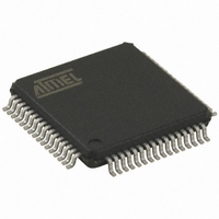
IC 8051 MCU 32K CRAM USB 64-VQFP
Manufacturer
Atmel
Series
89Cr
Datasheet
1.AT89C5122D-PSTUM.pdf
(208 pages)
Specifications of AT89C5122D-RDRUM
Core Processor
8051
Core Size
8-Bit
Speed
48MHz
Connectivity
SmartCard, SPI, UART/USART, USB
Peripherals
LED, POR, WDT
Number Of I /o
46
Program Memory Size
32KB (32K x 8)
Program Memory Type
FLASH
Ram Size
768 x 8
Voltage - Supply (vcc/vdd)
3 V ~ 5.5 V
Oscillator Type
Internal
Operating Temperature
-40°C ~ 85°C
Package / Case
64-TQFP, 64-VQFP
For Use With
AT89OCD-01 - USB EMULATOR FOR AT8XC51 MCUAT89STK-10 - KIT EVAL APPL MASS STORAGEAT89STK-03 - KIT STARTER FOR MCU AT8XC5122/23
Lead Free Status / RoHS Status
Lead free / RoHS Compliant
Eeprom Size
-
Data Converters
-
Other names
AT89C5122D-RDRUMTR
Available stocks
Company
Part Number
Manufacturer
Quantity
Price


Memory Organization
Program Memory
Managament
18
AT83R5122, AT8xC5122/23
The AT83R5122, AT8xC5122/23 devices have separated address spaces for Program
and Data Memory, as shown in Figure 12 on page 27, Figure 13 on page 29 and Figure
14 on page 30. The logical separation of Program and Data memory allows the Data
Memory to be accessed by 8-bit addresses, which can be more quickly stored and
manipulated by an-bit CPU. Nevertheless, 16-bit Data Memory addresses can also be
generated through the DPTR register.
Depending on the state of EA pin, the MCU fetches the code from internal or external
program memory (ROMless mode)
Warning : the EA pin can not be left floating, otherwise MCU may have an unpredict-
able behaviour.
If EA is strapped to VCC, the MCU fetches the code from the internal program memory.
The way the MCU works in this mode depends on the device version. See next para-
graphs for further details.
If the EA is strapped to GND, the MCU fetches the code from external program memory.
This mode is common for all device versions wich supports it. After reset, the CPU
begins the execution from location 0000h. There can be up to 64 KBytes of program
memory. In this mode, the internal program memories are disabled.
The hardware configuration for external program execution is shown in Figure 8.
Figure 8. Executing from External Program Memory
Note that the 16 I/O lines (Ports 0 and 2) are dedicated to bus functions during external
Program Memory fetches. Port 0 serves as a multiplexed address/dat bus. It emits the
low byte of the Program Counter (PCL) as an address, and then goes into a float state
awaiting the arrival of the code byte from the Program Memory. During the time that the
low byte of the Program Counter is valid on P0, the signal ALE (Address Latch Enable)
clocks the byte into an address latch. Meanwhile, Port 2 emits the high byte of the Pro-
gram Counter (PCH). Then PSEN strobes the External Program Memory and the code
byte is read into the MCU.
PSEN is not activated and Ports P0 and P2 are not affected during internal program
fetches.
AT8xC5122
PSEN#
ALE
P2
P0
AD7:0
A15:8
Latch
A7:0
EXTERNAL PROGRAM
A15:8
A7:0
D7:0
OE
MEMORY
4202F–SCR–07/2008
Related parts for AT89C5122D-RDRUM
Image
Part Number
Description
Manufacturer
Datasheet
Request
R


Part Number:
Description:
IC 8051 MCU W/SMART CARD 64VQFP
Manufacturer:
Atmel
Datasheet:

Part Number:
Description:
IC 8051 MCU FLASH 32K 64QFN
Manufacturer:
Atmel
Datasheet:
Part Number:
Description:
IC 8051 MCU FLASH 32K 64VQFP
Manufacturer:
Atmel
Datasheet:
Part Number:
Description:
IC MCU 80C51 W/SMART CARD 64VQFP
Manufacturer:
Atmel
Datasheet:

Part Number:
Description:
IC 8051 MCU FLASH 32K 28PLCC
Manufacturer:
Atmel
Datasheet:


Part Number:
Description:
MICROCONTROLLER WITH USB AND SMART CARD READER INTERFACES
Manufacturer:
ATMEL [ATMEL Corporation]
Datasheet:

Part Number:
Description:
KIT STARTER FOR MCU AT8XC5122/23
Manufacturer:
Atmel
Datasheet:

Part Number:
Description:
IC MICRO CTRL 24MHZ 44TQFP
Manufacturer:
Atmel
Datasheet:

Part Number:
Description:
IC MICRO CTRL 24MHZ 44PLCC
Manufacturer:
Atmel
Datasheet:
Part Number:
Description:
IC MICRO CTRL 24MHZ 44PLCC
Manufacturer:
Atmel
Datasheet:

Part Number:
Description:
IC MICRO CTRL 24MHZ 40DIP
Manufacturer:
Atmel
Datasheet: