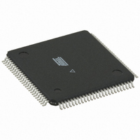
ATMEGA3250PV-10AU Atmel, ATMEGA3250PV-10AU Datasheet - Page 51

ATMEGA3250PV-10AU
Manufacturer Part Number
ATMEGA3250PV-10AU
Description
IC MCU AVR 32K FLASH 100-TQFP
Manufacturer
Atmel
Series
AVR® ATmegar
Datasheet
1.ATMEGA3250P-20AU.pdf
(364 pages)
Specifications of ATMEGA3250PV-10AU
Core Processor
AVR
Core Size
8-Bit
Speed
10MHz
Connectivity
SPI, UART/USART, USI
Peripherals
Brown-out Detect/Reset, POR, PWM, WDT
Number Of I /o
69
Program Memory Size
32KB (16K x 16)
Program Memory Type
FLASH
Eeprom Size
1K x 8
Ram Size
2K x 8
Voltage - Supply (vcc/vdd)
1.8 V ~ 5.5 V
Data Converters
A/D 8x10b
Oscillator Type
Internal
Operating Temperature
-40°C ~ 85°C
Package / Case
100-TQFP, 100-VQFP
Processor Series
ATMEGA32x
Core
AVR8
Data Bus Width
8 bit
Data Ram Size
2 KB
Interface Type
SPI, UART, USI
Maximum Clock Frequency
10 MHz
Number Of Programmable I/os
69
Number Of Timers
3
Maximum Operating Temperature
+ 85 C
Mounting Style
SMD/SMT
Minimum Operating Temperature
- 40 C
On-chip Adc
10 bit, 8 Channel
Data Rom Size
1 KB
Operating Supply Voltage
1.8 V to 5.5 V
Operating Temperature Range
- 40 C to + 85 C
A/d Bit Size
10 bit
A/d Channels Available
8
Height
1 mm
Length
14 mm
Supply Voltage (max)
5.5 V
Supply Voltage (min)
1.8 V
Width
14 mm
For Use With
ATSTK600-TQFP100 - STK600 SOCKET/ADAPTER 100-TQFP770-1007 - ISP 4PORT ATMEL AVR MCU SPI/JTAG770-1005 - ISP 4PORT FOR ATMEL AVR MCU JTAG770-1004 - ISP 4PORT FOR ATMEL AVR MCU SPIATAVRISP2 - PROGRAMMER AVR IN SYSTEMATSTK504 - STARTER KIT AVR EXP MOD 100P LCD
Lead Free Status / RoHS Status
Lead free / RoHS Compliant
Other names
ATMEGA3250PV-8AU
ATMEGA3250PV-8AU
ATMEGA3250PV-8AU
Available stocks
Company
Part Number
Manufacturer
Quantity
Price
- Current page: 51 of 364
- Download datasheet (6Mb)
10.5.2
8023F–AVR–07/09
WDTCR – Watchdog Timer Control Register
• Bits 7:5 – Res: Reserved Bits
These bits are reserved and will always read as zero.
• Bit 4 – WDCE: Watchdog Change Enable
This bit must be set when the WDE bit is written to logic zero. Otherwise, the Watchdog will not
be disabled. Once written to one, hardware will clear this bit after four clock cycles. Refer to the
description of the WDE bit for a Watchdog disable procedure. This bit must also be set when
changing the prescaler bits. See
Watchdog Timer” on page
• Bit 3 – WDE: Watchdog Enable
When the WDE is written to logic one, the Watchdog Timer is enabled, and if the WDE is written
to logic zero, the Watchdog Timer function is disabled. WDE can only be cleared if the WDCE bit
has logic level one. To disable an enabled Watchdog Timer, the following procedure must be
followed:
1. In the same operation, write a logic one to WDCE and WDE. A logic one must be written
2. Within the next four clock cycles, write a logic 0 to WDE. This disables the Watchdog.
In safety level 2, it is not possible to disable the Watchdog Timer, even with the algorithm
described above.
• Bits 2:0 – WDP2, WDP1, WDP0: Watchdog Timer Prescaler 2, 1, and 0
The WDP2, WDP1, and WDP0 bits determine the Watchdog Timer prescaling when the Watch-
dog Timer is enabled. The different prescaling values and their corresponding Time-out Periods
are shown in
Table 10-2.
Bit
(0x60)
Read/Write
Initial Value
WDP2
to WDE even though it is set to one before the disable operation starts.
0
0
0
0
1
1
1
1
WDP1
Table 10-2 on page
0
0
1
1
0
0
1
1
Watchdog Timer Prescale Select
R
7
–
0
See Section “10.4.1” on page 49.
WDP0
0
1
0
1
0
1
0
1
R
6
–
0
49.
Oscillator Cycles
Number of WDT
51.
1,024K cycles
2,048K cycles
128K cycles
256K cycles
512K cycles
R
”Timed Sequences for Changing the Configuration of the
16K cycles
32K cycles
64K cycles
5
–
0
WDCE
R/W
4
0
WDE
R/W
3
0
Typical Time-out at
ATmega325P/3250P
V
CC
17.1 ms
34.3 ms
68.5 ms
0.14 s
0.27 s
0.55 s
WDP2
1.1 s
2.2 s
R/W
= 3.0V
2
0
WDP1
R/W
1
0
Typical Time-out at
WDP0
R/W
V
0
0
CC
16.3 ms
32.5 ms
65 ms
0.13 s
0.26 s
0.52 s
1.0 s
2.1 s
= 5.0V
WDTCR
51
Related parts for ATMEGA3250PV-10AU
Image
Part Number
Description
Manufacturer
Datasheet
Request
R

Part Number:
Description:
Manufacturer:
Atmel Corporation
Datasheet:

Part Number:
Description:
IC AVR MCU 32K 16MHZ 100TQFP
Manufacturer:
Atmel
Datasheet:

Part Number:
Description:
IC AVR MCU 32K 16MHZ 100TQFP
Manufacturer:
Atmel
Datasheet:

Part Number:
Description:
MCU AVR 32K FLASH 16MHZ 100TQFP
Manufacturer:
Atmel
Datasheet:

Part Number:
Description:
Atmega3250 8-bit Microcontroller With In-system Programmable Flash
Manufacturer:
ATMEL Corporation

Part Number:
Description:
Manufacturer:
Atmel Corporation
Datasheet:

Part Number:
Description:
IC AVR MCU 32K 16MHZ 64-QFN
Manufacturer:
Atmel
Datasheet:

Part Number:
Description:
IC AVR MCU 32K 16MHZ 64TQFP
Manufacturer:
Atmel
Datasheet:

Part Number:
Description:
IC AVR MCU 32K 16MHZ 64TQFP
Manufacturer:
Atmel
Datasheet:

Part Number:
Description:
IC AVR MCU 32K 16MHZ 64-QFN
Manufacturer:
Atmel
Datasheet:

Part Number:
Description:
8-bit Microcontroller with In-System Programmable Flash
Manufacturer:
ATMEL [ATMEL Corporation]
Datasheet:

Part Number:
Description:
MCU AVR 32K FLASH 16MHZ 64TQFP
Manufacturer:
Atmel
Datasheet:

Part Number:
Description:
MCU AVR 32K FLASH 16MHZ 64QFN
Manufacturer:
Atmel
Datasheet:


