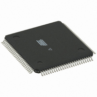
ATMEGA3250PV-10AU Atmel, ATMEGA3250PV-10AU Datasheet - Page 72

ATMEGA3250PV-10AU
Manufacturer Part Number
ATMEGA3250PV-10AU
Description
IC MCU AVR 32K FLASH 100-TQFP
Manufacturer
Atmel
Series
AVR® ATmegar
Datasheet
1.ATMEGA3250P-20AU.pdf
(364 pages)
Specifications of ATMEGA3250PV-10AU
Core Processor
AVR
Core Size
8-Bit
Speed
10MHz
Connectivity
SPI, UART/USART, USI
Peripherals
Brown-out Detect/Reset, POR, PWM, WDT
Number Of I /o
69
Program Memory Size
32KB (16K x 16)
Program Memory Type
FLASH
Eeprom Size
1K x 8
Ram Size
2K x 8
Voltage - Supply (vcc/vdd)
1.8 V ~ 5.5 V
Data Converters
A/D 8x10b
Oscillator Type
Internal
Operating Temperature
-40°C ~ 85°C
Package / Case
100-TQFP, 100-VQFP
Processor Series
ATMEGA32x
Core
AVR8
Data Bus Width
8 bit
Data Ram Size
2 KB
Interface Type
SPI, UART, USI
Maximum Clock Frequency
10 MHz
Number Of Programmable I/os
69
Number Of Timers
3
Maximum Operating Temperature
+ 85 C
Mounting Style
SMD/SMT
Minimum Operating Temperature
- 40 C
On-chip Adc
10 bit, 8 Channel
Data Rom Size
1 KB
Operating Supply Voltage
1.8 V to 5.5 V
Operating Temperature Range
- 40 C to + 85 C
A/d Bit Size
10 bit
A/d Channels Available
8
Height
1 mm
Length
14 mm
Supply Voltage (max)
5.5 V
Supply Voltage (min)
1.8 V
Width
14 mm
For Use With
ATSTK600-TQFP100 - STK600 SOCKET/ADAPTER 100-TQFP770-1007 - ISP 4PORT ATMEL AVR MCU SPI/JTAG770-1005 - ISP 4PORT FOR ATMEL AVR MCU JTAG770-1004 - ISP 4PORT FOR ATMEL AVR MCU SPIATAVRISP2 - PROGRAMMER AVR IN SYSTEMATSTK504 - STARTER KIT AVR EXP MOD 100P LCD
Lead Free Status / RoHS Status
Lead free / RoHS Compliant
Other names
ATMEGA3250PV-8AU
ATMEGA3250PV-8AU
ATMEGA3250PV-8AU
Available stocks
Company
Part Number
Manufacturer
Quantity
Price
- Current page: 72 of 364
- Download datasheet (6Mb)
PCINT12, Pin Change Interrupt Source 12: The PB4 pin can serve as an external interrupt
source.
• MISO/PCINT11 – Port B, Bit 3
MISO: Master Data input, Slave Data output pin for SPI. When the SPI is enabled as a Master,
this pin is configured as an input regardless of the setting of DDB3. When the SPI is enabled as
a Slave, the data direction of this pin is controlled by DDB3. When the pin is forced to be an
input, the pull-up can still be controlled by the PORTB3 bit.
PCINT11, Pin Change Interrupt Source 11: The PB3 pin can serve as an external interrupt
source.
• MOSI/PCINT10 – Port B, Bit 2
MOSI: SPI Master Data output, Slave Data input for SPI. When the SPI is enabled as a Slave,
this pin is configured as an input regardless of the setting of DDB2. When the SPI is enabled as
a Master, the data direction of this pin is controlled by DDB2. When the pin is forced to be an
input, the pull-up can still be controlled by the PORTB2 bit.
PCINT10, Pin Change Interrupt Source 10: The PB2 pin can serve as an external interrupt
source.
• SCK/PCINT9 – Port B, Bit 1
SCK: Master Clock output, Slave Clock input pin for SPI. When the SPI is enabled as a Slave,
this pin is configured as an input regardless of the setting of DDB1. When the SPI is enabled as
a Master, the data direction of this pin is controlled by DDB1. When the pin is forced to be an
input, the pull-up can still be controlled by the PORTB1 bit.
PCINT9, Pin Change Interrupt Source 9: The PB1 pin can serve as an external interrupt source.
• SS/PCINT8 – Port B, Bit 0
SS: Slave Port Select input. When the SPI is enabled as a Slave, this pin is configured as an
input regardless of the setting of DDB0. As a Slave, the SPI is activated when this pin is driven
low. When the SPI is enabled as a Master, the data direction of this pin is controlled by DDB0.
When the pin is forced to be an input, the pull-up can still be controlled by the PORTB0 bit
PCINT8, Pin Change Interrupt Source 8: The PB0 pin can serve as an external interrupt source.
ATmega325P/3250P
72
8023F–AVR–07/09
Related parts for ATMEGA3250PV-10AU
Image
Part Number
Description
Manufacturer
Datasheet
Request
R

Part Number:
Description:
Manufacturer:
Atmel Corporation
Datasheet:

Part Number:
Description:
IC AVR MCU 32K 16MHZ 100TQFP
Manufacturer:
Atmel
Datasheet:

Part Number:
Description:
IC AVR MCU 32K 16MHZ 100TQFP
Manufacturer:
Atmel
Datasheet:

Part Number:
Description:
MCU AVR 32K FLASH 16MHZ 100TQFP
Manufacturer:
Atmel
Datasheet:

Part Number:
Description:
Atmega3250 8-bit Microcontroller With In-system Programmable Flash
Manufacturer:
ATMEL Corporation

Part Number:
Description:
Manufacturer:
Atmel Corporation
Datasheet:

Part Number:
Description:
IC AVR MCU 32K 16MHZ 64-QFN
Manufacturer:
Atmel
Datasheet:

Part Number:
Description:
IC AVR MCU 32K 16MHZ 64TQFP
Manufacturer:
Atmel
Datasheet:

Part Number:
Description:
IC AVR MCU 32K 16MHZ 64TQFP
Manufacturer:
Atmel
Datasheet:

Part Number:
Description:
IC AVR MCU 32K 16MHZ 64-QFN
Manufacturer:
Atmel
Datasheet:

Part Number:
Description:
8-bit Microcontroller with In-System Programmable Flash
Manufacturer:
ATMEL [ATMEL Corporation]
Datasheet:

Part Number:
Description:
MCU AVR 32K FLASH 16MHZ 64TQFP
Manufacturer:
Atmel
Datasheet:

Part Number:
Description:
MCU AVR 32K FLASH 16MHZ 64QFN
Manufacturer:
Atmel
Datasheet:


