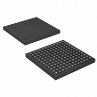
AT91SAM7L128-CU Atmel, AT91SAM7L128-CU Datasheet - Page 272

AT91SAM7L128-CU
Manufacturer Part Number
AT91SAM7L128-CU
Description
MCU ARM7 128K HS FLASH 144-LFBGA
Manufacturer
Atmel
Series
AT91SAMr
Datasheet
1.AT91SAM7L64-CU.pdf
(564 pages)
Specifications of AT91SAM7L128-CU
Core Processor
ARM7
Core Size
16/32-Bit
Speed
36MHz
Connectivity
I²C, SPI, UART/USART
Peripherals
Brown-out Detect/Reset, LCD, POR, PWM, WDT
Number Of I /o
80
Program Memory Size
128KB (128K x 8)
Program Memory Type
FLASH
Ram Size
6K x 8
Voltage - Supply (vcc/vdd)
1.55 V ~ 1.8 V
Data Converters
A/D 4x10b
Oscillator Type
Internal
Operating Temperature
-40°C ~ 85°C
Package / Case
144-LFBGA
Processor Series
AT91SAMx
Core
ARM7TDMI
Data Bus Width
32 bit
Data Ram Size
6 KB
Interface Type
2-Wire, SPI, USART
Maximum Clock Frequency
36 MHz
Number Of Programmable I/os
80
Number Of Timers
3
Maximum Operating Temperature
+ 85 C
Mounting Style
SMD/SMT
3rd Party Development Tools
JTRACE-ARM-2M, MDK-ARM, RL-ARM, ULINK2
Development Tools By Supplier
AT91SAM-ICE, AT91-ISP, AT91SAM7L-EK
Minimum Operating Temperature
- 40 C
On-chip Adc
10 bit, 4 Channel
For Use With
AT91SAM7L-STK - KIT EVAL FOR AT91SAM7LAT91SAM-ICE - EMULATOR FOR AT91 ARM7/ARM9
Lead Free Status / RoHS Status
Lead free / RoHS Compliant
Eeprom Size
-
Lead Free Status / Rohs Status
Details
Available stocks
Company
Part Number
Manufacturer
Quantity
Price
Company:
Part Number:
AT91SAM7L128-CU
Manufacturer:
Atmel
Quantity:
2 660
- Current page: 272 of 564
- Download datasheet (9Mb)
27.4.5
27.4.6
27.4.7
272
AT91SAM7L128/64 Preliminary
Synchronous Data Output
Multi Drive Control (Open Drain)
Output Line Timings
The results of these write operations are detected in PIO_OSR (Output Status Register). When
a bit in this register is at 0, the corresponding I/O line is used as an input only. When the bit is at
1, the corresponding I/O line is driven by the PIO controller.
The level driven on an I/O line can be determined by writing in PIO_SODR (Set Output Data
Register) and PIO_CODR (Clear Output Data Register). These write operations respectively set
and clear PIO_ODSR (Output Data Status Register), which represents the data driven on the I/O
lines. Writing in PIO_OER and PIO_ODR manages PIO_OSR whether the pin is configured to
be controlled by the PIO controller or assigned to a peripheral function. This enables configura-
tion of the I/O line prior to setting it to be managed by the PIO Controller.
Similarly, writing in PIO_SODR and PIO_CODR effects PIO_ODSR. This is important as it
defines the first level driven on the I/O line.
Controlling all parallel busses using several PIOs requires two successive write operations in the
PIO_SODR and PIO_CODR registers. This may lead to unexpected transient values. The PIO
controller offers a direct control of PIO outputs by single write access to PIO_ODSR (Output
Data Status Register). Only bits unmasked by PIO_OWSR (Output Write Status Register) are
written. The mask bits in the PIO_OWSR are set by writing to PIO_OWER (Output Write Enable
Register) and cleared by writing to PIO_OWDR (Output Write Disable Register).
After reset, the synchronous data output is disabled on all the I/O lines as PIO_OWSR resets at
0x0.
Each I/O can be independently programmed in Open Drain by using the Multi Drive feature. This
feature permits several drivers to be connected on the I/O line which is driven low only by each
device. An external pull-up resistor (or enabling of the internal one) is generally required to guar-
antee a high level on the line.
The Multi Drive feature is controlled by PIO_MDER (Multi-driver Enable Register) and
PIO_MDDR (Multi-driver Disable Register). The Multi Drive can be selected whether the I/O line
is controlled by the PIO controller or assigned to a peripheral function. PIO_MDSR (Multi-driver
Status Register) indicates the pins that are configured to support external drivers.
After reset, the Multi Drive feature is disabled on all pins, i.e. PIO_MDSR resets at value 0x0.
Figure 27-4
directly writing PIO_ODSR. This last case is valid only if the corresponding bit in PIO_OWSR is
set.
Figure 27-4
shows how the outputs are driven either by writing PIO_SODR or PIO_CODR, or by
also shows when the feedback in PIO_PDSR is available.
6257A–ATARM–20-Feb-08
Related parts for AT91SAM7L128-CU
Image
Part Number
Description
Manufacturer
Datasheet
Request
R

Part Number:
Description:
KIT EVAL FOR AT91SAM7L
Manufacturer:
Atmel
Datasheet:

Part Number:
Description:
DEV KIT FOR AVR/AVR32
Manufacturer:
Atmel
Datasheet:

Part Number:
Description:
INTERVAL AND WIPE/WASH WIPER CONTROL IC WITH DELAY
Manufacturer:
ATMEL Corporation
Datasheet:

Part Number:
Description:
Low-Voltage Voice-Switched IC for Hands-Free Operation
Manufacturer:
ATMEL Corporation
Datasheet:

Part Number:
Description:
MONOLITHIC INTEGRATED FEATUREPHONE CIRCUIT
Manufacturer:
ATMEL Corporation
Datasheet:

Part Number:
Description:
AM-FM Receiver IC U4255BM-M
Manufacturer:
ATMEL Corporation
Datasheet:

Part Number:
Description:
Monolithic Integrated Feature Phone Circuit
Manufacturer:
ATMEL Corporation
Datasheet:

Part Number:
Description:
Multistandard Video-IF and Quasi Parallel Sound Processing
Manufacturer:
ATMEL Corporation
Datasheet:

Part Number:
Description:
High-performance EE PLD
Manufacturer:
ATMEL Corporation
Datasheet:

Part Number:
Description:
8-bit Flash Microcontroller
Manufacturer:
ATMEL Corporation
Datasheet:

Part Number:
Description:
2-Wire Serial EEPROM
Manufacturer:
ATMEL Corporation
Datasheet:


