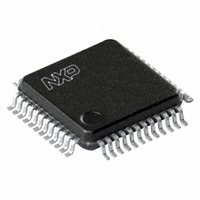
LPC1343FBD48,151 NXP Semiconductors, LPC1343FBD48,151 Datasheet - Page 9

LPC1343FBD48,151
Manufacturer Part Number
LPC1343FBD48,151
Description
IC MCU 32BIT 32KB FLASH 48LQFP
Manufacturer
NXP Semiconductors
Series
LPC13xxr
Specifications of LPC1343FBD48,151
Program Memory Type
FLASH
Program Memory Size
32KB (32K x 8)
Package / Case
48-LQFP
Core Processor
ARM® Cortex-M3™
Core Size
32-Bit
Speed
72MHz
Connectivity
I²C, Microwire, SPI, SSI, SSP, UART/USART, USB
Peripherals
Brown-out Detect/Reset, POR, WDT
Number Of I /o
40
Ram Size
8K x 8
Voltage - Supply (vcc/vdd)
2 V ~ 3.6 V
Data Converters
A/D 8x10b
Oscillator Type
Internal
Operating Temperature
-40°C ~ 85°C
Processor Series
LPC13
Core
ARM Cortex M3
Data Bus Width
32 bit
Data Ram Size
8 KB
Interface Type
I2C, UART
Maximum Clock Frequency
72 MHz
Number Of Programmable I/os
42
Number Of Timers
4
Operating Supply Voltage
3.3 V
Maximum Operating Temperature
+ 85 C
Mounting Style
SMD/SMT
3rd Party Development Tools
MDK-ARM, RL-ARM, ULINK2, KSK-LPC1343
Development Tools By Supplier
OM11039, OM11040, OM11046, OM11048
Minimum Operating Temperature
- 40 C
On-chip Adc
10 bit, 8 Channel
Cpu Family
LPC1000
Device Core
ARM Cortex-M3
Device Core Size
32b
Frequency (max)
72MHz
Total Internal Ram Size
8KB
# I/os (max)
42
Number Of Timers - General Purpose
4
Operating Supply Voltage (typ)
3.3V
Operating Supply Voltage (max)
3.6V
Operating Supply Voltage (min)
2V
Instruction Set Architecture
RISC
Operating Temp Range
-40C to 85C
Operating Temperature Classification
Industrial
Mounting
Surface Mount
Pin Count
48
Package Type
LQFP
Lead Free Status / RoHS Status
Lead free / RoHS Compliant
For Use With
622-1005 - USB IN-CIRCUIT PROG ARM7 LPC2K
Eeprom Size
-
Lead Free Status / Rohs Status
Lead free / RoHS Compliant
Other names
568-4945
935289652151
935289652151
Available stocks
Company
Part Number
Manufacturer
Quantity
Price
Company:
Part Number:
LPC1343FBD48,151
Manufacturer:
NXP Semiconductors
Quantity:
10 000
Part Number:
LPC1343FBD48,151
Manufacturer:
NXP/恩智浦
Quantity:
20 000
NXP Semiconductors
Table 3.
LPC1311_13_42_43
Product data sheet
Symbol
RESET/PIO0_0
PIO0_1/CLKOUT/
CT32B0_MAT2/
USB_FTOGGLE
PIO0_2/SSEL/
CT16B0_CAP0
PIO0_3/USB_VBUS 14
PIO0_4/SCL
PIO0_5/SDA
PIO0_6/
USB_CONNECT/
SCK
PIO0_7/CTS
PIO0_8/MISO/
CT16B0_MAT0
PIO0_9/MOSI/
CT16B0_MAT1/
SWO
LPC1313/43 LQFP48 pin description table
6.2 Pin description
Pin
3
4
10
15
16
22
23
27
28
[2]
[3]
[3]
[3]
[4]
[4]
[3]
[3]
[3]
[3]
Start
logic
input
yes
yes
yes
yes
yes
yes
yes
yes
yes
yes
Type Reset
I
I/O
I/O
O
O
O
I/O
I/O
I
I/O
I
I/O
I/O
I/O
I/O
I/O
O
I/O
I/O
I
I/O
I/O
O
I/O
I/O
O
O
All information provided in this document is subject to legal disclaimers.
state
[1]
I; PU
-
I; PU
-
-
-
I; PU
-
-
I; PU
-
I; IA
-
I; IA
-
I; PU
-
-
I; PU
-
I; PU
-
-
I; PU
-
-
-
Rev. 3 — 10 August 2010
Description
RESET — External reset input: A LOW on this pin resets the device,
causing I/O ports and peripherals to take on their default states, and
processor execution to begin at address 0.
PIO0_0 — General purpose digital input/output pin.
PIO0_1 — General purpose digital input/output pin. A LOW level on
this pin during reset starts the ISP command handler or the USB device
enumeration (USB on LPC1343 only, see description of PIO0_3).
CLKOUT — Clockout pin.
CT32B0_MAT2 — Match output 2 for 32-bit timer 0.
USB_FTOGGLE — USB 1 ms Start-of-Frame signal (LPC1343 only).
PIO0_2 — General purpose digital input/output pin.
SSEL — Slave select for SSP.
CT16B0_CAP0 — Capture input 0 for 16-bit timer 0.
PIO0_3 — General purpose digital input/output pin. LPC1343 only: A
LOW level on this pin during reset starts the ISP command handler, a
HIGH level starts the USB device enumeration.
USB_VBUS — Monitors the presence of USB bus power (LPC1343
only).
PIO0_4 — General purpose digital input/output pin (open-drain).
SCL — I
if I
PIO0_5 — General purpose digital input/output pin (open-drain).
SDA — I
I
PIO0_6 — General purpose digital input/output pin.
USB_CONNECT — Signal used to switch an external 1.5 kΩ resistor
under software control. Used with the SoftConnect USB feature
(LPC1343 only).
SCK — Serial clock for SSP.
PIO0_7 — General purpose digital input/output pin (high-current output
driver).
CTS — Clear To Send input for UART.
PIO0_8 — General purpose digital input/output pin.
MISO — Master In Slave Out for SSP.
CT16B0_MAT0 — Match output 0 for 16-bit timer 0.
PIO0_9 — General purpose digital input/output pin.
MOSI — Master Out Slave In for SSP.
CT16B0_MAT1 — Match output 1 for 16-bit timer 0.
SWO — Serial wire trace output.
2
C Fast-mode Plus is selected in the I/O configuration register.
2
C Fast-mode Plus is selected in the I/O configuration register.
2
2
C-bus clock input/output (open-drain). High-current sink only
C-bus data input/output (open-drain). High-current sink only if
32-bit ARM Cortex-M3 microcontroller
LPC1311/13/42/43
© NXP B.V. 2010. All rights reserved.
9 of 62


