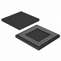
LPC3131FET180,551 NXP Semiconductors, LPC3131FET180,551 Datasheet - Page 49

LPC3131FET180,551
Manufacturer Part Number
LPC3131FET180,551
Description
IC ARM9 MCU 180MHZ 180-TFBGA
Manufacturer
NXP Semiconductors
Series
LPC3000r
Datasheet
1.OM11024.pdf
(72 pages)
Specifications of LPC3131FET180,551
Package / Case
180-TFBGA
Core Processor
ARM9
Core Size
32-Bit
Speed
180MHz
Connectivity
EBI/EMI, I²C, MMC, SPI, UART/USART, USB OTG
Peripherals
DMA, I²S, LCD, PWM, WDT
Program Memory Type
ROMless
Ram Size
192K x 8
Voltage - Supply (vcc/vdd)
1.1 V ~ 3.6 V
Data Converters
A/D 4x10b
Oscillator Type
External
Operating Temperature
-40°C ~ 85°C
Processor Series
LPC31
Core
ARM926EJ-S
Data Bus Width
16 bit, 32 bit
Data Ram Size
192 KB
Interface Type
I2C/I2S/UART/USB
Maximum Clock Frequency
180 MHz
Number Of Timers
4
Operating Supply Voltage
2.7 V to 3.6 V
Maximum Operating Temperature
+ 85 C
Mounting Style
SMD/SMT
3rd Party Development Tools
MDK-ARM, RL-ARM, ULINK2, KSK-LPC3131-PL
Development Tools By Supplier
OM11028
Minimum Operating Temperature
- 40 C
On-chip Adc
4-ch x 10-bit
Lead Free Status / RoHS Status
Lead free / RoHS Compliant
For Use With
568-4850 - KIT EVAL FOR LPC313X568-4062 - DEBUGGER J-LINK JTAG568-4061 - DEBUGGER U-LINK2 JTAG FOR NXP
Number Of I /o
-
Eeprom Size
-
Program Memory Size
-
Lead Free Status / Rohs Status
Lead free / RoHS Compliant
Other names
568-4697
935288014551
LPC3131FET180-S
935288014551
LPC3131FET180-S
Available stocks
Company
Part Number
Manufacturer
Quantity
Price
Company:
Part Number:
LPC3131FET180,551
Manufacturer:
NXP Semiconductors
Quantity:
10 000
NXP Semiconductors
Table 18.
C
[1]
[2]
[3]
[4]
[5]
[6]
LPC3130_3131
Preliminary data sheet
Symbol
Common to read and write cycles
t
Read cycle parameters
t
t
t
t
t
t
t
t
t
t
t
t
Write cycle parameters
t
t
t
t
t
t
t
t
t
t
CSLAV
OELAV
BLSLAV
CSLOEL
CSLBLSL
OELOEH
BLSLBLSH
su(D)
h(D)
CSHOEH
CSHBLSH
OEHANV
BLSHANV
CSLDV
CSLWEL
CSLBLSL
WELDV
WELWEH
BLSLBLSH
WEHANV
WEHDNV
BLSHANV
BLSHDNV
L
= 25 pF, T
Refer to the LPC3130/3131 user manual for the programming of WAITOEN and HCLK.
Refer to the LPC3130/3131 user manual for the programming of WAITRD and HCLK.
(WAITRD − WAITOEN + 1) = 3 min at 60 MHz.
Refer to the LPC3130/3131 user manual for the programming of WAITWEN and HCLK.
Refer to the LPC3130/3131 user manual for the programming of WAITWR and HCLK.
(WAITWD − WAITWEN + 1) = 3 min at 60 MHz.
Dynamic characteristics: static external memory interface
Parameter
CS LOW to address valid
time
OE LOW to address valid
time
BLS LOW to address valid
time
CS LOW to OE LOW time
CS LOW to BLS LOW time
OE LOW to OE HIGH time
BLS LOW to BLS HIGH time
data input set-up time
data input hold time
CS HIGH to OE HIGH time
CS HIGH to BLS HIGH time
OE HIGH to address invalid
time
BLS HIGH to address invalid
time
CS LOW to data valid time
CS LOW to WE LOW time
CS LOW to BLS LOW time
WE LOW to data valid time
WE LOW to WE HIGH time
BLS LOW to BLS HIGH time
WE HIGH to address invalid
time
WE HIGH to data invalid time
BLS HIGH to address invalid
time
BLS HIGH to data invalid
time
amb
=
9.2 SRAM controller
−
40
°
C to +85
°
C, unless otherwise specified; V
All information provided in this document is subject to legal disclaimers.
Conditions
Rev. 1.04 — 27 May 2010
[1][2][3]
[1][2][3]
[4][5][6]
[4][5]
[1]
[1]
[1]
[4]
[4]
[4]
Low-cost, low-power ARM926EJ-S microcontrollers
Min
−1.8
-
-
-
-
-
-
9
-
3
-
10
-
-
-
-
-
-
-
-
-
-
-
DD(IO)
Typ
0
0 − WAITOEN × HCLK
0 − WAITOEN × HCLK
0 + WAITOEN × HCLK
0 + WAITOEN × HCLK
(WAITRD − WAITOEN + 1) × HCLK
(WAITRD − WAITOEN + 1) × HCLK
-
0
0
0
-
1 × HCLK
-
(WAITWEN + 1) × HCLK
WAITWEN × HCLK
0 − (WAITWEN + 1) × HCLK
(WAITWR − WAITWEN + 1) × HCLK
(WAITWR − WAITWEN + 3) × HCLK
1 × HCLK
1 × HCLK
1 × HCLK
1 × HCLK
= 1.8 V and 3.3 V (SUP8).
LPC3130/3131
© NXP B.V. 2010. All rights reserved.
Max
4
-
-
-
-
-
-
-
-
-
-
-
-
9
-
-
-
-
-
-
-
-
-
49 of 72
Unit
ns
ns
ns
ns
ns
ns
ns
ns
ns
ns
ns
ns
ns
ns
ns
ns
ns
ns
ns
ns
ns
ns
ns


