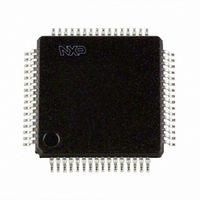
LPC2109FBD64/01,15 NXP Semiconductors, LPC2109FBD64/01,15 Datasheet - Page 22

LPC2109FBD64/01,15
Manufacturer Part Number
LPC2109FBD64/01,15
Description
IC ARM7 MCU FLASH 64K 64-LQFP
Manufacturer
NXP Semiconductors
Series
LPC2100r
Datasheet
1.LPC2109FBD640115.pdf
(44 pages)
Specifications of LPC2109FBD64/01,15
Program Memory Type
FLASH
Program Memory Size
64KB (64K x 8)
Package / Case
64-LQFP
Core Processor
ARM7
Core Size
16/32-Bit
Speed
60MHz
Connectivity
CAN, I²C, Microwire, SPI, SSI, SSP, UART/USART
Peripherals
POR, PWM, WDT
Number Of I /o
46
Ram Size
8K x 8
Voltage - Supply (vcc/vdd)
1.65 V ~ 3.6 V
Data Converters
A/D 4x10b
Oscillator Type
Internal
Operating Temperature
-40°C ~ 85°C
Processor Series
LPC21
Core
ARM7TDMI-S
Data Bus Width
16 bit, 32 bit
Data Ram Size
8 KB
Interface Type
CAN/I2C/JTAG/SPI/SSP/UART
Maximum Clock Frequency
60 MHz
Number Of Programmable I/os
46
Number Of Timers
2
Operating Supply Voltage
1.8 V
Maximum Operating Temperature
+ 85 C
Mounting Style
SMD/SMT
3rd Party Development Tools
MDK-ARM, RL-ARM, ULINK2
Minimum Operating Temperature
- 40 C
On-chip Adc
4-ch x 10-bit
Package
64LQFP
Device Core
ARM7TDMI-S
Family Name
LPC2000
Maximum Speed
60 MHz
Lead Free Status / RoHS Status
Lead free / RoHS Compliant
For Use With
568-4310 - EVAL BOARD LPC2158 W/LCD568-4297 - BOARD EVAL LPC21XX MCB2100622-1005 - USB IN-CIRCUIT PROG ARM7 LPC2K
Eeprom Size
-
Lead Free Status / Rohs Status
Lead free / RoHS Compliant
Other names
568-4311
935284891151
LPC2109FBD64/01-S
LPC2109FBD64/01-S
935284891151
LPC2109FBD64/01-S
LPC2109FBD64/01-S
Available stocks
Company
Part Number
Manufacturer
Quantity
Price
Company:
Part Number:
LPC2109FBD64/01,15
Manufacturer:
NXP Semiconductors
Quantity:
10 000
NXP Semiconductors
Product data sheet
LPC2109_2119_2129_6
CAUTION
6.18.5 External interrupt inputs
6.18.6 Memory mapping control
6.18.7 Power control
CRP1 disables access to chip via the JTAG and allows partial flash update (excluding
flash sector 0) using a limited set of the ISP commands. This mode is useful when CRP is
required and flash field updates are needed but all sectors can not be erased.
CRP2 disables access to chip via the JTAG and only allows full flash erase and update
using a reduced set of the ISP commands.
Running an application with level CRP3 selected fully disables any access to chip via the
JTAG pins and the ISP. This mode effectively disables ISP override using P0[14] pin, too. It
is up to the user’s application to provide (if needed) flash update mechanism using IAP
calls or call reinvoke ISP command to enable flash update via UART0.
Remark: Devices without the suffix /00 or /01 have only a security level equivalent to
CRP2 available.
The LPC2109/2119/2129 include up to nine edge or level sensitive External Interrupt
Inputs as selectable pin functions. When the pins are combined, external events can be
processed as four independent interrupt signals. The External Interrupt Inputs can
optionally be used to wake up the processor from Power-down mode.
The Memory Mapping Control alters the mapping of the interrupt vectors that appear
beginning at address 0x0000 0000. Vectors may be mapped to the bottom of the on-chip
flash memory, or to the on-chip static RAM. This allows code running in different memory
spaces to have control of the interrupts.
The LPC2109/2119/2129 support two reduced power modes: Idle mode and Power-down
mode. In Idle mode, execution of instructions is suspended until either a Reset or interrupt
occurs. Peripheral functions continue operation during Idle mode and may generate
interrupts to cause the processor to resume execution. Idle mode eliminates power used
by the processor itself, memory systems and related controllers, and internal buses.
In Power-down mode, the oscillator is shut down and the chip receives no internal clocks.
The processor state and registers, peripheral registers, and internal SRAM values are
preserved throughout Power-down mode and the logic levels of chip output pins remain
static. The Power-down mode can be terminated and normal operation resumed by either
a Reset or certain specific interrupts that are able to function without clocks. Since all
dynamic operation of the chip is suspended, Power-down mode reduces chip power
consumption to nearly zero.
A Power Control for Peripherals feature allows individual peripherals to be turned off if
they are not needed in the application, resulting in additional power savings.
If level three Code Read Protection (CRP3) is selected, no future factory testing can be
performed on the device.
Rev. 06 — 10 December 2007
LPC2109/2119/2129
Single-chip 16/32-bit microcontrollers
© NXP B.V. 2007. All rights reserved.
22 of 44


