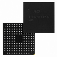
LPC3220FET296/01,5 NXP Semiconductors, LPC3220FET296/01,5 Datasheet - Page 6

LPC3220FET296/01,5
Manufacturer Part Number
LPC3220FET296/01,5
Description
IC ARM9 MCU 128K 296-TFBGA
Manufacturer
NXP Semiconductors
Series
LPC32x0r
Specifications of LPC3220FET296/01,5
Package / Case
296-TFBGA
Core Processor
ARM9
Core Size
16/32-Bit
Speed
266MHz
Connectivity
EBI/EMI, I²C, IrDA, Microwire, SPI, SSI, SSP, UART/USART, USB OTG
Peripherals
DMA, I²S, Motor Control PWM, PWM, WDT
Number Of I /o
51
Program Memory Type
ROMless
Ram Size
128K x 8
Voltage - Supply (vcc/vdd)
0.9 V ~ 3.6 V
Data Converters
A/D 3x10b
Oscillator Type
Internal
Operating Temperature
-40°C ~ 85°C
Processor Series
LPC32
Core
ARM926EJ-S
Data Bus Width
32 bit
Data Ram Size
128 KB
Interface Type
EMC
Maximum Clock Frequency
266 MHz
Number Of Timers
6
Operating Supply Voltage
1.31 V to 1.39 V
Maximum Operating Temperature
+ 85 C
Mounting Style
SMD/SMT
3rd Party Development Tools
MDK-ARM, RL-ARM, ULINK2
Minimum Operating Temperature
- 40 C
On-chip Adc
10 bit, 3 Channel
Lead Free Status / RoHS Status
Lead free / RoHS Compliant
Eeprom Size
-
Program Memory Size
-
Lead Free Status / Rohs Status
Lead free / RoHS Compliant
Other names
568-4965
935290763551
935290763551
Available stocks
Company
Part Number
Manufacturer
Quantity
Price
Company:
Part Number:
LPC3220FET296/01,5
Manufacturer:
NXP Semiconductors
Quantity:
10 000
NXP Semiconductors
ES_LPC3220
Errata sheet
3.2 NOR.1: When booting from NOR flash, SDRAM devices will not
Work-around:
When interfacing an external peripheral device that does not support burst mode access
through the EMC Static Memory interface the following work-arounds are recommended:
release the data bus, preventing the LPC3220 from booting correctly
Introduction:
In systems that use SDRAM and boot from NOR FLASH, an issue can occur on system
reset that will prevent the SDRAM devices from releasing the data bus. This will prevent
normal operation of NOR FLASH due to data bus contention and prevent the LPC3220
from booting correctly. This applies to systems using either Single Data Rate (SDR) or
Double Data Rate (DDR) SDRAM devices.
Problem:
If the LPC3220 is reset during an SDRAM access, the SDRAM clock and clock enable will
be immediately de-asserted. If the de-assertion occurs during the period of time the
SDRAM is driving the data bus, the SDRAM will hold that state until the next clock occurs
at the SDRAM clock input when the clock enable is active. However, the LPC3220 won't
deliver the clock and clock enables until software actually sets up the EMC state to do
this, so the SDRAM will remain in the data assertion state on the data bus while the
LPC3220 tries to boot.
When the chip attempts to load boot code from NOR FLASH after reset, the correct
signals are asserted to the NOR FLASH device and the NOR FLASH device places its
data on the data bus. But if the SDRAM is still driving the bus, the NOR FLASH device
and SDRAM device are in contention and the data will not be read correctly into the
LPC3220. In this situation, the LPC3220 will fail to boot.
Work-around:
Since this issue only occurs with NOR FLASH, using one of the other boot methods such
as NAND or SPI FLASH boot is a good workaround for the issue.
If booting from NOR FLASH is a requirement, the simple circuit shown in
used to clear the SDRAM state at system reset. This will not change the normal
functioning of the LPC3220 EMC or SDRAM operations. If SDRAM devices are also
present on the 2nd SDRAM chip select, a similar circuit will be needed for those devices
using EMC_CKE1.
1. Avoid using DMA to transfer read blocks of data from the external device. Instead use
2. If DMA can't be avoided, ensure there is at least one unused address between the
a software loop with LDR instruction to read blocks of data from the external device.
highest address used for the external device DMA data buffer and any status or
control register in the device that will initiate any unwanted action just by reading from
the register (i.e. clear an interrupt or status).
All information provided in this document is subject to legal disclaimers.
Rev. 8 — 1 February 2011
ES_LPC3220
Errata sheet LPC3220
© NXP B.V. 2011. All rights reserved.
Figure 3
can be
6 of 16


