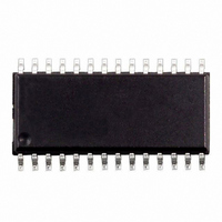
ST72F264G2M6 STMicroelectronics, ST72F264G2M6 Datasheet - Page 158

ST72F264G2M6
Manufacturer Part Number
ST72F264G2M6
Description
IC MCU 8BIT 8K 28 SOIC
Manufacturer
STMicroelectronics
Series
ST7r
Datasheet
1.STEVAL-ISQ002V1.pdf
(172 pages)
Specifications of ST72F264G2M6
Core Processor
ST7
Core Size
8-Bit
Speed
16MHz
Connectivity
I²C, SCI, SPI
Peripherals
LVD, POR, PWM, WDT
Number Of I /o
22
Program Memory Size
8KB (8K x 8)
Program Memory Type
FLASH
Ram Size
256 x 8
Voltage - Supply (vcc/vdd)
2.7 V ~ 5.5 V
Data Converters
A/D 6x10b
Oscillator Type
Internal
Operating Temperature
-40°C ~ 85°C
Package / Case
28-SOIC (7.5mm Width)
Processor Series
ST72F2x
Core
ST7
Data Bus Width
8 bit
Data Ram Size
256 B
Interface Type
I2C/SCI/SPI
Maximum Clock Frequency
8 MHz
Number Of Programmable I/os
22
Number Of Timers
3
Operating Supply Voltage
2.7 V to 5.5 V
Maximum Operating Temperature
+ 85 C
Mounting Style
SMD/SMT
Development Tools By Supplier
ST7F264-IND/USB, ST72F34X-SK/RAIS, ST7MDT10-DVP3, ST7MDT10-EMU3, STX-RLINK
Minimum Operating Temperature
- 40 C
On-chip Adc
6-ch x 10-bit
Controller Family/series
ST7
No. Of I/o's
22
Ram Memory Size
256Byte
Cpu Speed
8MHz
No. Of Timers
2
Embedded Interface Type
I2C, SCI, SPI
Rohs Compliant
Yes
For Use With
497-6423 - BOARD EVAL BASED ON ST72264G1497-5046 - KIT TOOL FOR ST7/UPSD/STR7 MCU
Lead Free Status / RoHS Status
Lead free / RoHS Compliant
Eeprom Size
-
Lead Free Status / Rohs Status
Lead free / RoHS Compliant
Other names
497-2106-5
Available stocks
Company
Part Number
Manufacturer
Quantity
Price
Company:
Part Number:
ST72F264G2M6
Manufacturer:
SCS
Quantity:
1 225
Part Number:
ST72F264G2M6
Manufacturer:
ST
Quantity:
20 000
ST72260Gx, ST72262Gx, ST72264Gx
ADC CHARACTERISTICS (Cont’d)
13.12.0.1 General PCB Design Guidelines
To obtain best results, some general design and
layout rules should be followed when designing
the application PCB to shield the noise-sensitive,
analog physical interface from noise generating
CMOS logic signals.
– Properly place components and route the signal
ADC Accuracy with f
Figure 100. ADC Accuracy Characteristics
Notes:
1. ADC Accuracy vs. Negative Injection Current: Injecting negative current on any of the analog input pins significantly
reduces the accuracy of the conversion being performed on another analog input.
For I
for each 10KΩ increase of the external analog source impedance. It is recommended to add a Schottky diode (pin to
ground) to analog pins which may potentially inject negative current. Any positive injection current within the limits spec-
ified for I
2. Refer to
158/172
Symbol
1023
1022
1021
traces on the PCB to shield the analog inputs.
|E
|E
|E
|E
|E
7
6
5
4
3
2
1
INJ-
0
O
G
D
T
L
V
|
|
|
|
|
=0.8mA, the typical leakage induced inside the die is 1.6µA and the effect on the ADC accuracy is a loss of 4 LSB
SS
INJ(PIN)
Digital Result ADCDR
“Typical values” on page 126
1LSB
1
Total unadjusted error
Offset error
Gain Error
Differential linearity error
Integral linearity error
E
O
and ΣI
2
IDEAL
3
Parameter
INJ(PIN)
1)
=
1)
CPU
V
------------------------------- -
4
DD
1024
=8 MHz, f
in
–
5
1 LSB
V
Section 13.8
SS
1)
1)
E
6
T
IDEAL
1)
E
7
L
for more information on typical ADC accuracy values.
ADC
(2)
=4 MHz R
does not affect the ADC accuracy.
Conditions
E
D
1021 1022 1023 1024
(3)
AIN
(1)
< 10
E
G
Analog signals paths should run over the analog
ground plane and be as short as possible. Isolate
analog signals from digital signals that may
switch while the analog inputs are being sampled
by the A/D converter. Do not toggle digital out-
puts on the same I/O port as the A/D input being
converted.
Typ
kΩ,
V
1.5
4
1
1
3
DD
2)
V
FLASH
(1) Example of an actual transfer curve
(2) The ideal transfer curve
(3) End point correlation line
E
between the actual and the ideal transfer curves.
E
transition and the first ideal one.
E
transition and the last actual one.
E
between actual steps and the ideal one.
E
between any actual transition and the end point
correlation line.
DD
T
O
G
D
L
=Total Unadjusted Error: maximum deviation
=Integral Linearity Error: maximum deviation
=Offset Error: deviation between the first actual
=Gain Error: deviation between the last ideal
=Differential Linearity Error: maximum deviation
= 4.5V to 5.5V
V
Max
in
4.5
4.5
4.5
6
5
(LSB
IDEAL
Typ
)
TBD
TBD
TBD
TBD
TBD
2)
ROM
Max
TBD
TBD
TBD
TBD
TBD
Unit
LSB


