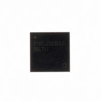
CY8CLED03D02-56LTXI Cypress Semiconductor Corp, CY8CLED03D02-56LTXI Datasheet - Page 22

CY8CLED03D02-56LTXI
Manufacturer Part Number
CY8CLED03D02-56LTXI
Description
IC POWERPSOC 3CH 1A 56VQFN
Manufacturer
Cypress Semiconductor Corp
Series
PowerPSoC® CY8CLEDr
Datasheet
1.CY8CLED03D02-56LTXI.pdf
(47 pages)
Specifications of CY8CLED03D02-56LTXI
Core Processor
M8C
Core Size
8-Bit
Speed
24MHz
Connectivity
DALI, DMX512, I²C, IrDA, SPI, UART/USART
Peripherals
LED, LVD, POR, PWM, WDT
Number Of I /o
14
Program Memory Size
16KB (16K x 8)
Program Memory Type
FLASH
Ram Size
1K x 8
Voltage - Supply (vcc/vdd)
4.75 V ~ 5.25 V
Oscillator Type
Internal
Operating Temperature
-40°C ~ 85°C
Package / Case
56-VQFN Exposed Pad, 56-HVQFN, 56-SQFN, 56-DHVQFN
Lead Free Status / RoHS Status
Lead free / RoHS Compliant
For Use With
428-2882 - KIT STARTER POWERPSOC LIGHTING428-2281 - KIT EVAL POWERPSOC LIGHTING428-2271 - KIT EVAL COLOR-LOCK428-2270 - KIT STARTER DEMO LIGHTING770-1000 - ISP 4PORT FOR CYPRESS PSOC MCU
Eeprom Size
-
Data Converters
-
Lead Free Status / Rohs Status
Details
Other names
428-2925
Available stocks
Company
Part Number
Manufacturer
Quantity
Price
Company:
Part Number:
CY8CLED03D02-56LTXI
Manufacturer:
Cypress
Quantity:
128
13. Register General Conventions
13.1 Abbreviations Used
The register conventions specific to this section are listed in
Table
Table 13-1. Register Conventions
Document Number: 001-46319 Rev. *E
R
W
L
C
#
Convention
13-1.
Read register or bit(s)
Write register or bit(s)
Logical register or bit(s)
Clearable register or bit(s)
Access is bit specific
Description
13.2 Register Naming Conventions
The register naming convention specific to the PSoC core
section of PowerPSoC blocks and their registers is:
Therefore, ASD13CR3 is a register for an analog PowerPSoC
block in row 1 column 3.
The register naming convention specific to the power peripheral
section of PowerPSoC blocks and their registers is:
Therefore, CSA0_CR is a register for a power peripheral
PowerPSoC block in for Current Sense Amplifier, channel 0.
13.3 Register Mapping Tables
The PowerPSoC device has a total register address space of
512 bytes. The register space is also referred to as I/O space and
is broken into two parts. The XIO bit in the Flag register (CPU_F)
determines which bank the user is currently in. When the XIO bit
is set, the user is said to be in the “extended” address space or
the “configuration” registers.
More detailed description of the Registers are found in the
PowerPSoC TRM.
CY8CLED04G01, CY8CLED03G01
CY8CLED04D01, CY8CLED04D02
CY8CLED03D01, CY8CLED03D02
where m = row index, n = column index
where x = number of channel
<Prefix>mn<Suffix>
<Prefix>x<Suffix>
Page 22 of 47
[+] Feedback


