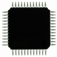
C8051F501-IQ Silicon Laboratories Inc, C8051F501-IQ Datasheet - Page 182

C8051F501-IQ
Manufacturer Part Number
C8051F501-IQ
Description
IC 8051 MCU 64K FLASH 48-QFP
Manufacturer
Silicon Laboratories Inc
Series
C8051F50xr
Specifications of C8051F501-IQ
Program Memory Type
FLASH
Program Memory Size
64KB (64K x 8)
Package / Case
48-QFP
Mfg Application Notes
LIN Bootloader AppNote
Core Processor
8051
Core Size
8-Bit
Speed
50MHz
Connectivity
EBI/EMI, SMBus (2-Wire/I²C), SPI, UART/USART
Peripherals
POR, PWM, Temp Sensor, WDT
Number Of I /o
40
Ram Size
4.25K x 8
Voltage - Supply (vcc/vdd)
1.8 V ~ 5.25 V
Data Converters
A/D 32x12b
Oscillator Type
Internal
Operating Temperature
-40°C ~ 125°C
Processor Series
C8051F5x
Core
8051
Data Bus Width
8 bit
Data Ram Size
4.25 KB
Interface Type
I2C/SPI/UART
Maximum Clock Frequency
50 MHz
Number Of Programmable I/os
40
Number Of Timers
4
Maximum Operating Temperature
+ 125 C
Mounting Style
SMD/SMT
3rd Party Development Tools
PK51, CA51, A51, ULINK2
Development Tools By Supplier
C8051F500DK
Minimum Operating Temperature
- 40 C
On-chip Adc
32-ch x 12-bit
Package
48PQFP
Device Core
8051
Family Name
C8051F50x
Maximum Speed
50 MHz
Operating Supply Voltage
2.5|3.3|5 V
Lead Free Status / RoHS Status
Lead free / RoHS Compliant
For Use With
336-1527 - KIT DEV FOR C8051F50X
Eeprom Size
-
Lead Free Status / Rohs Status
Lead free / RoHS Compliant
Other names
336-1512
Available stocks
Company
Part Number
Manufacturer
Quantity
Price
Company:
Part Number:
C8051F501-IQ
Manufacturer:
Silicon Laboratories Inc
Quantity:
10 000
Company:
Part Number:
C8051F501-IQR
Manufacturer:
Silicon Laboratories Inc
Quantity:
10 000
- Current page: 182 of 312
- Download datasheet (3Mb)
C8051F50x/F51x
20.4. Port I/O Initialization
Port I/O initialization consists of the following steps:
1. Select the input mode (analog or digital) for all Port pins, using the Port Input Mode register (PnMDIN).
2. Select the output mode (open-drain or push-pull) for all Port pins, using the Port Output Mode register
3. Select any pins to be skipped by the I/O Crossbar using the Port Skip registers (PnSKIP).
4. Assign Port pins to desired peripherals.
5. Enable the Crossbar (XBARE = 1).
All Port pins must be configured as either analog or digital inputs. Port 4 on the C8051F500/1/4/5 and
C8051F508/9-F510/1 is a digital-only Port. Any pins to be used as Comparator or ADC inputs should be
configured as an analog inputs. When a pin is configured as an analog input, its weak pullup, digital driver,
and digital receiver are disabled. This process saves power and reduces noise on the analog input. Pins
configured as digital inputs may still be used by analog peripherals; however this practice is not recom-
mended.
Additionally, all analog input pins should be configured to be skipped by the Crossbar (accomplished by
setting the associated bits in PnSKIP). Port input mode is set in the PnMDIN register, where a 1 indicates a
182
P o rt
S p e cia l
F u n ctio n
S ig n a ls
P IN I/O
UART _T X
UART _RX
CAN_T X
CAN_RX
S CK
M IS O
M O S I
NS S
S DA
S CL
CP 0
CP 0A
CP 1
CP 1A
S YS CL K
CEX 0
CEX 1
CEX 2
CEX 3
CEX 4
CEX 5
ECI
T 0
T 1
L IN_T X
L IN_RX
(PnMDOUT).
0
0
1
1
P 0S KIP [0:7]
2
1
Figure 20.4. Crossbar Priority Decoder in Example Configuration
3
0
P 0
4
0
5
1
6
0
7
0
0
0
1
0
*NS S Is only pinned out in 4-wire S P I M ode
P 1S KIP [0:7]
2
0
3
0
P 1
4
0
5
0
6
0
7
0
0
0
Rev. 1.2
1
0
P 2S KIP [0:7]
2
0
3
0
P 2
4
0
5
0
6
0
7
0
0
0
1
0
available on the 48-pin
P 3.1-P 3.7, P 4.0 only
and 40-pin pac k ages
P 3S KIP [0:7]
2
0
3
0
P 3
4
0
5
0
6
0
7
0
0
1
available on the 48-
P 4.1-P 4.7 only
2
pin pac k ages
3
P 4
4
5
6
7
Related parts for C8051F501-IQ
Image
Part Number
Description
Manufacturer
Datasheet
Request
R
Part Number:
Description:
SMD/C°/SINGLE-ENDED OUTPUT SILICON OSCILLATOR
Manufacturer:
Silicon Laboratories Inc
Part Number:
Description:
Manufacturer:
Silicon Laboratories Inc
Datasheet:
Part Number:
Description:
N/A N/A/SI4010 AES KEYFOB DEMO WITH LCD RX
Manufacturer:
Silicon Laboratories Inc
Datasheet:
Part Number:
Description:
N/A N/A/SI4010 SIMPLIFIED KEY FOB DEMO WITH LED RX
Manufacturer:
Silicon Laboratories Inc
Datasheet:
Part Number:
Description:
N/A/-40 TO 85 OC/EZLINK MODULE; F930/4432 HIGH BAND (REV E/B1)
Manufacturer:
Silicon Laboratories Inc
Part Number:
Description:
EZLink Module; F930/4432 Low Band (rev e/B1)
Manufacturer:
Silicon Laboratories Inc
Part Number:
Description:
I°/4460 10 DBM RADIO TEST CARD 434 MHZ
Manufacturer:
Silicon Laboratories Inc
Part Number:
Description:
I°/4461 14 DBM RADIO TEST CARD 868 MHZ
Manufacturer:
Silicon Laboratories Inc
Part Number:
Description:
I°/4463 20 DBM RFSWITCH RADIO TEST CARD 460 MHZ
Manufacturer:
Silicon Laboratories Inc
Part Number:
Description:
I°/4463 20 DBM RADIO TEST CARD 868 MHZ
Manufacturer:
Silicon Laboratories Inc
Part Number:
Description:
I°/4463 27 DBM RADIO TEST CARD 868 MHZ
Manufacturer:
Silicon Laboratories Inc
Part Number:
Description:
I°/4463 SKYWORKS 30 DBM RADIO TEST CARD 915 MHZ
Manufacturer:
Silicon Laboratories Inc
Part Number:
Description:
N/A N/A/-40 TO 85 OC/4463 RFMD 30 DBM RADIO TEST CARD 915 MHZ
Manufacturer:
Silicon Laboratories Inc
Part Number:
Description:
I°/4463 20 DBM RADIO TEST CARD 169 MHZ
Manufacturer:
Silicon Laboratories Inc


