R5F212B7SNFP#U0 Renesas Electronics America, R5F212B7SNFP#U0 Datasheet - Page 142
R5F212B7SNFP#U0
Manufacturer Part Number
R5F212B7SNFP#U0
Description
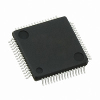
IC R8C/2B MCU FLASH 64-LQFP
Manufacturer
Renesas Electronics America
Series
R8C/2x/2Br
Specifications of R5F212B7SNFP#U0
Core Processor
R8C
Core Size
16/32-Bit
Speed
20MHz
Connectivity
I²C, LIN, SIO, SSU, UART/USART
Peripherals
POR, PWM, Voltage Detect, WDT
Number Of I /o
55
Program Memory Size
48KB (48K x 8)
Program Memory Type
FLASH
Ram Size
2.5K x 8
Voltage - Supply (vcc/vdd)
2.2 V ~ 5.5 V
Data Converters
A/D 12x10b; D/A 2x8b
Oscillator Type
Internal
Operating Temperature
-20°C ~ 85°C
Package / Case
64-LQFP
For Use With
R0K5212D8S001BE - KIT STARTER FOR R8C/2DR0K5212D8S000BE - KIT DEV FOR R8C/2D
Lead Free Status / RoHS Status
Lead free / RoHS Compliant
Eeprom Size
-
Available stocks
Company
Part Number
Manufacturer
Quantity
Price


R8C/2A Group, R8C/2B Group
Rev.2.00
REJ09B0324-0200
10.7
10.7.1
10.7.2
10.7.3
10.7.4
When entering stop mode, set the FMR01 bit in the FMR0 register to 0 (CPU rewrite mode disabled) and the
CM10 bit in the CM1 register to 1 (stop mode). An instruction queue pre-reads 4 bytes from the instruction
which sets the CM10 bit to 1 (stop mode) and the program stops.
Insert at least 4 NOP instructions following the JMP.B instruction after the instruction which sets the CM10 bit
to 1.
• Program example to enter stop mode
When entering wait mode, set the FMR01 bit in the FMR0 register to 0 (CPU rewrite mode disabled) and
execute the WAIT instruction. An instruction queue pre-reads 4 bytes from the WAIT instruction and the
program stops. Insert at least 4 NOP instructions after the WAIT instruction.
• Program example to execute the WAIT instruction
Since the oscillation stop detection function cannot be used if the XIN clock frequency is 2 MHz or below, set
bits OCD1 to OCD0 to 00b.
Ask the manufacturer of the oscillator to specify the best oscillation circuit constants for your system.
To use this MCU with supply voltage below VCC = 2.7 V, it is recommended to set the CM11 bit in the CM1
register to 1 (on-chip feedback resistor disabled), the CM15 bit to 1 (high drive capacity), and connect the
feedback resistor to the chip externally.
Notes on Clock Generation Circuit
Nov 26, 2007
Stop Mode
Wait Mode
Oscillation Stop Detection Function
Oscillation Circuit Constants
Page 120 of 580
LABEL_001 :
BCLR
BSET
FSET
BSET
JMP.B
NOP
NOP
NOP
NOP
BCLR
FSET
WAIT
NOP
NOP
NOP
NOP
1,FMR0
0,PRCR
I
0,CM1
LABEL_001
1,FMR0
I
; CPU rewrite mode disabled
; Protect disabled
; Enable interrupt
; Stop mode
; CPU rewrite mode disabled
; Enable interrupt
; Wait mode
10. Clock Generation Circuit
Related parts for R5F212B7SNFP#U0
Image
Part Number
Description
Manufacturer
Datasheet
Request
R

Part Number:
Description:
KIT STARTER FOR M16C/29
Manufacturer:
Renesas Electronics America
Datasheet:

Part Number:
Description:
KIT STARTER FOR R8C/2D
Manufacturer:
Renesas Electronics America
Datasheet:

Part Number:
Description:
R0K33062P STARTER KIT
Manufacturer:
Renesas Electronics America
Datasheet:

Part Number:
Description:
KIT STARTER FOR R8C/23 E8A
Manufacturer:
Renesas Electronics America
Datasheet:

Part Number:
Description:
KIT STARTER FOR R8C/25
Manufacturer:
Renesas Electronics America
Datasheet:

Part Number:
Description:
KIT STARTER H8S2456 SHARPE DSPLY
Manufacturer:
Renesas Electronics America
Datasheet:

Part Number:
Description:
KIT STARTER FOR R8C38C
Manufacturer:
Renesas Electronics America
Datasheet:

Part Number:
Description:
KIT STARTER FOR R8C35C
Manufacturer:
Renesas Electronics America
Datasheet:

Part Number:
Description:
KIT STARTER FOR R8CL3AC+LCD APPS
Manufacturer:
Renesas Electronics America
Datasheet:
Part Number:
Description:
KIT STARTER FOR RX610
Manufacturer:
Renesas Electronics America
Datasheet:

Part Number:
Description:
KIT STARTER FOR R32C/118
Manufacturer:
Renesas Electronics America
Datasheet:

Part Number:
Description:
KIT DEV RSK-R8C/26-29
Manufacturer:
Renesas Electronics America
Datasheet:

Part Number:
Description:
KIT STARTER FOR SH7124
Manufacturer:
Renesas Electronics America
Datasheet:

Part Number:
Description:
KIT STARTER FOR H8SX/1622
Manufacturer:
Renesas Electronics America
Datasheet:

Part Number:
Description:
KIT DEV FOR SH7203
Manufacturer:
Renesas Electronics America
Datasheet: