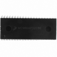
MC908AP32CBE Freescale Semiconductor, MC908AP32CBE Datasheet - Page 233

MC908AP32CBE
Manufacturer Part Number
MC908AP32CBE
Description
IC MCU 32K FLASH 8MHZ 42DIP
Manufacturer
Freescale Semiconductor
Series
HC08r
Specifications of MC908AP32CBE
Core Processor
HC08
Core Size
8-Bit
Speed
8MHz
Connectivity
I²C, IRSCI, SCI, SPI
Peripherals
LED, LVD, POR, PWM
Number Of I /o
30
Program Memory Size
32KB (32K x 8)
Program Memory Type
FLASH
Ram Size
2K x 8
Voltage - Supply (vcc/vdd)
2.7 V ~ 5.5 V
Data Converters
A/D 8x10b
Oscillator Type
Internal
Operating Temperature
-40°C ~ 85°C
Package / Case
42-DIP (0.600", 15.24mm)
Controller Family/series
HC08
No. Of I/o's
30
Ram Memory Size
2KB
Cpu Speed
8MHz
No. Of Timers
2
Embedded Interface Type
I2C, SCI, SPI
Rohs Compliant
Yes
Processor Series
HC08AP
Core
HC08
Data Bus Width
8 bit
Data Ram Size
2 KB
Interface Type
SCI, SPI
Maximum Clock Frequency
8 MHz
Number Of Programmable I/os
32
Number Of Timers
4
Maximum Operating Temperature
+ 85 C
Mounting Style
Through Hole
Development Tools By Supplier
FSICEBASE, DEMO908AP64E, M68CBL05CE
Minimum Operating Temperature
- 40 C
On-chip Adc
10 bit, 8 Channel
Lead Free Status / RoHS Status
Lead free / RoHS Compliant
Eeprom Size
-
Lead Free Status / Rohs Status
Details
- Current page: 233 of 324
- Download datasheet (4Mb)
14.5 Multi-Master IIC Bus Protocol
Normally a standard communication is composed of four parts:
These are described briefly in the following sections and illustrated in
14.5.1 START Signal
When the bus is free, (i.e. no master device is engaging the bus — both SCL and SDA lines are at logic
high) a master may initiate communication by sending a START signal. As shown in
START signal is defined as a high to low transition of SDA while SCL is high. This signal denotes the
beginning of a new data transfer (each data transfer may contain several bytes of data) and wakes up all
slaves.
14.5.2 Slave Address Transmission
The first byte transferred immediately after the START signal is the slave address transmitted by the
master. This is a 7-bit calling address followed by a R/W-bit. The R/W-bit dictates to the slave the desired
direction of the data transfer. A logic 0 indicates that the master wishes to transmit data to the slave; a
logic 1 indicates that the master wishes to receive data from the slave.
Freescale Semiconductor
1. START signal,
2. slave address transmission,
3. data transfer, and
4. STOP signal.
SDA
SDA
SCL
SCL
START
START
signal
signal
MSB
MSB
1
1
Figure 14-2. Multi-Master IIC Bus Transmission Signal Diagram
1
1
0
0
0
0
0
0
MC68HC908AP Family Data Sheet, Rev. 4
0
0
1
1
LSB
9th clock pulse
LSB
1
1
ACK
ACK
Repeated
START
signal
MSB
MSB
1
1
1
1
Data must be stable
when SCL is HIGH
0
0
Figure
1
1
14-2.
Multi-Master IIC Bus Protocol
0
0
0
0
Figure
1
1
9th clock pulse
LSB
LSB
1
1
No ACK
No ACK
14-2, a
STOP
signal
STOP
signal
231
Related parts for MC908AP32CBE
Image
Part Number
Description
Manufacturer
Datasheet
Request
R
Part Number:
Description:
Manufacturer:
Freescale Semiconductor, Inc
Datasheet:
Part Number:
Description:
Manufacturer:
Freescale Semiconductor, Inc
Datasheet:
Part Number:
Description:
Manufacturer:
Freescale Semiconductor, Inc
Datasheet:
Part Number:
Description:
Manufacturer:
Freescale Semiconductor, Inc
Datasheet:
Part Number:
Description:
Manufacturer:
Freescale Semiconductor, Inc
Datasheet:
Part Number:
Description:
Manufacturer:
Freescale Semiconductor, Inc
Datasheet:
Part Number:
Description:
Manufacturer:
Freescale Semiconductor, Inc
Datasheet:
Part Number:
Description:
Manufacturer:
Freescale Semiconductor, Inc
Datasheet:
Part Number:
Description:
Manufacturer:
Freescale Semiconductor, Inc
Datasheet:
Part Number:
Description:
Manufacturer:
Freescale Semiconductor, Inc
Datasheet:
Part Number:
Description:
Manufacturer:
Freescale Semiconductor, Inc
Datasheet:
Part Number:
Description:
Manufacturer:
Freescale Semiconductor, Inc
Datasheet:
Part Number:
Description:
Manufacturer:
Freescale Semiconductor, Inc
Datasheet:
Part Number:
Description:
Manufacturer:
Freescale Semiconductor, Inc
Datasheet:
Part Number:
Description:
Manufacturer:
Freescale Semiconductor, Inc
Datasheet:


