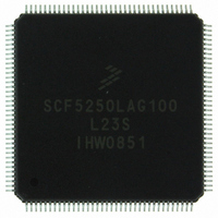
SCF5250LAG100 Freescale Semiconductor, SCF5250LAG100 Datasheet - Page 12

SCF5250LAG100
Manufacturer Part Number
SCF5250LAG100
Description
IC MPU COLDFIRE 100MHZ 144-LQFP
Manufacturer
Freescale Semiconductor
Series
SCF52xxr
Datasheet
1.SCFLXRAYADPTS12.pdf
(56 pages)
Specifications of SCF5250LAG100
Core Processor
Coldfire V2
Core Size
32-Bit
Speed
100MHz
Connectivity
EBI/EMI, I²C, IDE, MMC, SPI, UART/USART
Peripherals
DMA, I²S, POR, Serial Audio, WDT
Number Of I /o
57
Program Memory Type
ROMless
Ram Size
128K x 8
Voltage - Supply (vcc/vdd)
1.08 V ~ 1.32 V
Data Converters
A/D 6x12b
Oscillator Type
Internal
Operating Temperature
-20°C ~ 70°C
Package / Case
144-LQFP
Eeprom Size
-
Program Memory Size
-
Available stocks
Company
Part Number
Manufacturer
Quantity
Price
Company:
Part Number:
SCF5250LAG100
Manufacturer:
Intersil
Quantity:
90
Company:
Part Number:
SCF5250LAG100
Manufacturer:
Freescale Semiconductor
Quantity:
10 000
Part Number:
SCF5250LAG100
Manufacturer:
FREESCALE
Quantity:
20 000
Processor Status
Processor Clock
Test Clock
Test Reset/Development
Serial Clock
Test Mode Select/ Break
Point
Test Data Input /
Development Serial Input
Test Data
Output/Development
Serial Output
3.1
Many pins have an optional GPIO function.
3.2
These signals provide the external bus interface to the SCF5250 processor.
3.2.1
12
•
•
•
•
•
Signal Name
General purpose input is always active, regardless of state of pin.
General purpose output or primary output is determined by the appropriate setting of the Pin
Multiplex Control Registers, GPIO-FUNCTION, GPIO1-FUNCTION and PIN-CONFIG.
At Power-on reset, all pins are set to their primary function.
The address bus provides the address of the byte or most significant byte of the word or longword
being transferred. The address lines also serve as the DRAM address pins, providing multiplexed
row and column address signals.
Bits 23 down to 1 and 24 of the address are available. A24 is intended to be used with 256 Mbit
DRAM’s. Signals are named:
— A[23:1]
— A20/24
GPIO
SCF5250 Bus Signals
Address Bus
PST0/GPIO50
PST1/GPIO49
PST2/INTMON2/GPIO48
PST3/INTMON1/GPIO47
PSTCLK/GPIO51
TCK
TRST/DSCLK
TMS/BKPT
TDI/DSI
TDO/DSO
Table 2. SCF5250 Signal Index (continued)
SCF5250 Data Sheet:
Mnemonic
Technical
Indicates internal processor status.
processor clock output
Clock signal for IEEE 1149.1A JTAG.
Multiplexed signal that is asynchronous
reset for JTAG controller. Clock input for
debug module.
Multiplexed signal that is test mode select
in JTAG mode and a hardware
break-point in debug mode.
Multiplexed serial input for the JTAG or
background debug module.
Multiplexed serial output for the JTAG or
background debug module.
Data,
Rev. 1.3
Function
Freescale Semiconductor
Output
Input/
In/Out
Out
Out
In
In
In
In
Reset
State
Hi-Z
–
–
–
–
–
–


