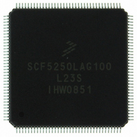
SCF5250LAG100 Freescale Semiconductor, SCF5250LAG100 Datasheet - Page 6

SCF5250LAG100
Manufacturer Part Number
SCF5250LAG100
Description
IC MPU COLDFIRE 100MHZ 144-LQFP
Manufacturer
Freescale Semiconductor
Series
SCF52xxr
Datasheet
1.SCFLXRAYADPTS12.pdf
(56 pages)
Specifications of SCF5250LAG100
Core Processor
Coldfire V2
Core Size
32-Bit
Speed
100MHz
Connectivity
EBI/EMI, I²C, IDE, MMC, SPI, UART/USART
Peripherals
DMA, I²S, POR, Serial Audio, WDT
Number Of I /o
57
Program Memory Type
ROMless
Ram Size
128K x 8
Voltage - Supply (vcc/vdd)
1.08 V ~ 1.32 V
Data Converters
A/D 6x12b
Oscillator Type
Internal
Operating Temperature
-20°C ~ 70°C
Package / Case
144-LQFP
Eeprom Size
-
Program Memory Size
-
Available stocks
Company
Part Number
Manufacturer
Quantity
Price
Company:
Part Number:
SCF5250LAG100
Manufacturer:
Intersil
Quantity:
90
Company:
Part Number:
SCF5250LAG100
Manufacturer:
Freescale Semiconductor
Quantity:
10 000
Part Number:
SCF5250LAG100
Manufacturer:
FREESCALE
Quantity:
20 000
1.2.16
The SCF5250 system bus allows connection of an IDE hard disk drive or SmartMedia flash card with a
minimum of external hardware. The external hardware consists of bus buffers for address and data and are
intended to reduce the load on the bus and prevent SDRAM and Flash accesses to propagate to the IDE
bus. The control signals for the buffers are generated in the SCF5250.
Low cost version SCF5250LPV100 and SCF5250LAG100 does not run production test for the
IDE/CF/SD/MMC interfaces. Freescale does not guarantee these interfaces will work on these two
devices.
1.2.17
The six channel ADC is a based on the Sigma-Delta concept with 12-bit resolution. Both the analogue
comparator and digital sections of the ADC are provided internally. An external integrator circuit
(resistor/capacitor) is required, which is driven by the ADC output. A software interrupt is provided when
the ADC measurement cycle is complete.
1.2.18
The two-wire I
serial bus that exchanges data between devices. The I
devices in the end system and is best suited for applications that need occasional bursts of rapid
communication over short distances among several devices. Bus capacitance and the number of unique
addresses limit the maximum communication length and the number of devices that can be connected.
1.2.19
Up to four programmable chip-select outputs provide signals that enable glueless connection to external
memory and peripheral circuits. The base address, access permissions and automatic wait-state insertion
are programmable with configuration registers. These signals also interface to 16-bit ports.
CS0 is active after reset to provide boot-up from external FLASH/ROM.
1.2.20
A total of 60 General Purpose inputs and 57 General Purpose outputs are available. These are multiplexed
with various other signals. Seven of the GPIO inputs have edge sensitive interrupt capability.
1.2.21
The interrupt controller provides user-programmable control of a total of 57 interrupts. There are 49
internal interrupt sources. In addition, there are 7 GPIOs where interrupts can be generated on the rising
or falling edge of the pin. All interrupts are autovectored and interrupt levels are programmable.
6
IDE and SmartMedia Interfaces
Analog/Digital Converter (ADC)
I
Chip-Selects
GPIO Interface
Interrupt Controller
2
C Module
2
C bus interface, which is compliant with the Philips I
SCF5250 Data Sheet:
Technical
2
C bus minimizes the interconnection between
Data,
Rev. 1.3
2
C bus standard, is a bidirectional
Freescale Semiconductor


