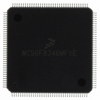
MC56F8346MFVE Freescale Semiconductor, MC56F8346MFVE Datasheet - Page 24

MC56F8346MFVE
Manufacturer Part Number
MC56F8346MFVE
Description
IC DSP 16BIT 60MHZ 144-LQFP
Manufacturer
Freescale Semiconductor
Series
56F8xxxr
Datasheet
1.MC56F8346VFVE.pdf
(178 pages)
Specifications of MC56F8346MFVE
Core Processor
56800
Core Size
16-Bit
Speed
60MHz
Connectivity
CAN, EBI/EMI, SCI, SPI
Peripherals
POR, PWM, Temp Sensor, WDT
Number Of I /o
62
Program Memory Size
136KB (68K x 16)
Program Memory Type
FLASH
Ram Size
6K x 16
Voltage - Supply (vcc/vdd)
2.25 V ~ 3.6 V
Data Converters
A/D 16x12b
Oscillator Type
External
Operating Temperature
-40°C ~ 125°C
Package / Case
144-LQFP
Data Bus Width
16 bit
Processor Series
MC56F83xx
Core
56800E
Numeric And Arithmetic Format
Fixed-Point
Device Million Instructions Per Second
60 MIPs
Maximum Clock Frequency
60 MHz
Number Of Programmable I/os
62
Data Ram Size
4 KB
Operating Supply Voltage
3.6 V
Maximum Operating Temperature
+ 125 C
Mounting Style
SMD/SMT
Interface Type
SCI, SPI, CAN
Minimum Operating Temperature
- 40 C
For Use With
MC56F8367EVME - EVAL BOARD FOR MC56F83X
Lead Free Status / RoHS Status
Lead free / RoHS Compliant
Eeprom Size
-
Lead Free Status / Rohs Status
Lead free / RoHS Compliant
Available stocks
Company
Part Number
Manufacturer
Quantity
Price
Company:
Part Number:
MC56F8346MFVE
Manufacturer:
Freescale
Quantity:
42
Company:
Part Number:
MC56F8346MFVE
Manufacturer:
Freescale Semiconductor
Quantity:
10 000
Part Number:
MC56F8346MFVE
Manufacturer:
FREESCALE
Quantity:
20 000
24
Signal Name
(GPIOF10)
(GPIOF11)
(GPIOF12)
(GPIOF13)
(GPIOF14)
(GPIOF15)
(GPIOF9)
GPIOB0
(A16)
D0
D1
D2
D3
D4
D5
D6
Table 2-2 Signal and Package Information for the 144 Pin LQFP
Pin No.
33
59
60
72
75
76
77
78
Schmitt
Outputt
Output
Output
Outpu
Input/
Input/
Input/
Type
disabled,
pull-up is
output is
enabled
In reset,
enabled
During
pull-up
56F8346 Technical Data, Rev. 15
Reset
Input,
State
Port B GPIO — This GPIO pin can be programmed as an input or
output pin.
Address Bus — A16 specifies one of the address lines for
external program or data memory accesses.
Depending upon the state of the DRV bit in the EMI bus control
register (BCR), A16 and EMI control signals are tri-stated when the
external bus is inactive.
Most designs will want to change the DRV state to DRV = 1 instead of
using the default setting.
After reset, the start-up state of GPIOB0 (GPIO or address) is
determined as a function of EXTBOOT, EMI_MODE and the Flash
security setting. See
pin is configured as an address pin at reset. In all cases, this state
may be changed by writing to GPIOB_PER.
To deactivate the internal pull-up resistor, clear bit 0 in the
GPIOB_PUR register.
Data Bus — D0 - D6 specify part of the data for external program or
data memory accesses.
Depending upon the state of the DRV bit in the EMI bus control
register (BCR), D0-D6 are tri-stated when the external bus is
inactive.
Most designs will want to change the DRV state to DRV = 1 instead of
using the default setting.
Port F GPIO — These seven GPIO pins can be individually
programmed as input or output pins.
At reset, these pins default to the EMI Data Bus function.
To deactivate the internal pull-up resistor, clear the appropriate
GPIO bit in the GPIOF_PUR register.
Example: GPIOF9, clear bit 9 in the GPIOF_PUR register.
Table 4-4
Signal Description
for further information on when this
Freescale Semiconductor
Preliminary


