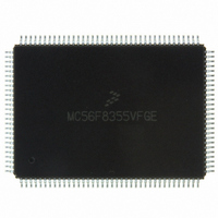
MC56F8355VFGE Freescale Semiconductor, MC56F8355VFGE Datasheet - Page 30

MC56F8355VFGE
Manufacturer Part Number
MC56F8355VFGE
Description
IC DSP 16BIT 60MHZ 128-LQFP
Manufacturer
Freescale Semiconductor
Series
56F8xxxr
Datasheet
1.MC56F8355VFGE.pdf
(172 pages)
Specifications of MC56F8355VFGE
Core Processor
56800
Core Size
16-Bit
Speed
60MHz
Connectivity
CAN, EBI/EMI, SCI, SPI
Peripherals
POR, PWM, Temp Sensor, WDT
Number Of I /o
49
Program Memory Size
264KB (132K x 16)
Program Memory Type
FLASH
Ram Size
10K x 16
Voltage - Supply (vcc/vdd)
2.25 V ~ 3.6 V
Data Converters
A/D 16x12b
Oscillator Type
External
Operating Temperature
-40°C ~ 105°C
Package / Case
128-LQFP
Data Bus Width
16 bit
Processor Series
MC56F83xx
Core
56800E
Numeric And Arithmetic Format
Fixed-Point
Device Million Instructions Per Second
60 MIPs
Maximum Clock Frequency
60 MHz
Number Of Programmable I/os
49
Data Ram Size
20 KB
Maximum Operating Temperature
+ 105 C
Mounting Style
SMD/SMT
Interface Type
SCI, SPI, CAN
Minimum Operating Temperature
- 40 C
For Use With
MC56F8367EVME - EVAL BOARD FOR MC56F83X
Lead Free Status / RoHS Status
Lead free / RoHS Compliant
Eeprom Size
-
Lead Free Status / Rohs Status
Lead free / RoHS Compliant
Available stocks
Company
Part Number
Manufacturer
Quantity
Price
Company:
Part Number:
MC56F8355VFGE
Manufacturer:
Freescale
Quantity:
562
Company:
Part Number:
MC56F8355VFGE
Manufacturer:
Freescale Semiconductor
Quantity:
10 000
Part Number:
MC56F8355VFGE
Manufacturer:
FREESCALE
Quantity:
20 000
30
Signal Name
(GPIOC10)
FAULTA0
FAULTA1
FAULTA2
FAULTA3
(GPIOC8)
(GPIOC9)
PWMA0
PWMA1
PWMA2
PWMA3
PWMA4
PWMA5
PWMB0
PWMB1
PWMB2
PWMB3
PWMB4
PWMB5
ISA0
ISA1
ISA2
Table 2-2 Signal and Package Information for the 128-Pin LQFP (Continued)
Pin No.
104
105
106
58
60
61
63
64
66
67
68
69
70
32
33
34
37
38
39
Schmitt
Schmitt
Schmitt
Output
Output
Output
Input/
Type
Input
Input
Input
output is
output is
In reset,
disabled
In reset,
disabled
enabled
enabled
enabled
During
56F8355 Technical Data, Rev. 17
Reset
pullup
pullup
pullup
State
Input,
Input,
Input,
PWMA0 - 5 — These are six PWMA outputs.
ISA0 - 2 — These three input current status pins are used for
top/bottom pulse width correction in complementary channel
operation for PWMA.
Port C GPIO — These GPIO pins can be individually programmed
as input or output pins.
In the 56F8355, these pins default to ISA functionality.
In the 56F8155, the default state is not one of the functions offered
and must be reconfigured.
To deactivate the internal pullup resistor, clear the appropriate bit
of the GPIOC_PUR register. See
FAULTA0 - A2 — These three fault input pins are used for
disabling selected PWMA outputs in cases where fault conditions
originate off-chip.
To deactivate the internal pullup resistor, set the PWMA0 bit in the
SIM_PUDR register. For details, see
FAULTA3 — This fault input pin is used for disabling selected
PWMA outputs in cases where fault conditions originate off-chip.
To deactivate the internal pullup resistor, set the PWMA1 bit in the
SIM_PUDR register. See
PWMB0 - 5 — Six PWMB output pins.
Signal Description
Part 6.5.6
Part 6.5.6
for details.
Part
6.5.6.
Freescale Semiconductor
for details.
Preliminary


