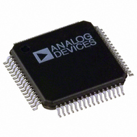
ADUC7128BSTZ126-RL Analog Devices Inc, ADUC7128BSTZ126-RL Datasheet - Page 36

ADUC7128BSTZ126-RL
Manufacturer Part Number
ADUC7128BSTZ126-RL
Description
IC DAS MCU ARM7 ADC/DDS 64-LQFP
Manufacturer
Analog Devices Inc
Series
MicroConverter® ADuC7xxxr
Datasheet
1.EVAL-ADUC7128QSPZ.pdf
(92 pages)
Specifications of ADUC7128BSTZ126-RL
Core Size
16/32-Bit
Program Memory Size
126KB (126K x 8)
Core Processor
ARM7
Speed
41.78MHz
Connectivity
I²C, SPI, UART/USART
Peripherals
PLA, POR, PWM, PSM, Temp Sensor, WDT
Number Of I /o
28
Program Memory Type
FLASH
Ram Size
8K x 8
Voltage - Supply (vcc/vdd)
3 V ~ 3.6 V
Data Converters
A/D 10x12b; D/A 1x10b
Oscillator Type
Internal
Operating Temperature
-40°C ~ 125°C
Package / Case
64-LQFP
Controller Family/series
(ARM7) ADUC
No. Of I/o's
40
Cpu Speed
41.78MHz
No. Of Timers
5
Digital Ic Case Style
LQFP
Embedded Interface Type
I2C, SPI, UART
Rohs Compliant
Yes
Lead Free Status / RoHS Status
Lead free / RoHS Compliant
For Use With
EVAL-ADUC7128QSPZ - KIT DEV FOR ADUC7128
Eeprom Size
-
Lead Free Status / RoHS Status
Lead free / RoHS Compliant, Lead free / RoHS Compliant
Other names
ADUC7128BSTZ126-RLTR
Available stocks
Company
Part Number
Manufacturer
Quantity
Price
Company:
Part Number:
ADUC7128BSTZ126-RL
Manufacturer:
Analog Devices Inc
Quantity:
10 000
ADuC7128/ADuC7129
CONVERTER OPERATION
The ADC incorporates a successive approximation (SAR)
architecture involving a charge-sampled input stage. This
architecture is described for the three different modes of
operation: differential mode, pseudo differential mode, and
single-ended mode.
Differential Mode
The ADuC7128/ADuC7129 contain a successive approximation
ADC based on two capacitive DACs. Figure 37 and Figure 38
show simplified schematics of the ADC in acquisition and
conversion phase, respectively. The ADC comprises control logic,
a SAR, and two capacitive DACs. In Figure 37 (the acquisition
phase), SW3 is closed and SW1 and SW2 are in Position A. The
comparator is held in a balanced condition, and the sampling
capacitor arrays acquire the differential signal on the input.
When the ADC starts a conversion (see Figure 38), SW3 opens
and SW1 and SW2 move to Position B, causing the comparator
to become unbalanced. Both inputs are disconnected once the
conversion begins. The control logic and the charge redistribution
DACs are used to add and subtract fixed amounts of charge
from the sampling capacitor arrays to bring the comparator
back into a balanced condition. When the comparator is
rebalanced, the conversion is complete. The control logic generates
the ADC output code. The output impedances of the sources
driving the V
the two inputs have different settling times, resulting in errors.
AIN13
AIN13
AIN0
AIN0
MUX
MUX
CHANNEL+
CHANNEL–
CHANNEL+
CHANNEL–
IN+
pin and the V
Figure 37. ADC Acquisition Phase
Figure 38. ADC Conversion Phase
B
A
A
B
B
A
A
B
V
V
REF
REF
SW1
SW2
SW1
SW2
C
C
IN−
C
C
S
S
S
S
pin must be matched; otherwise,
SW3
SW3
COMPARATOR
COMPARATOR
CAPACITIVE
CAPACITIVE
CAPACITIVE
CAPACITIVE
CONTROL
CONTROL
DAC
LOGIC
DAC
DAC
LOGIC
DAC
Rev. 0 | Page 36 of 92
Pseudo Differential Mode
In pseudo differential mode, Channel− is linked to the V
of the ADuC7128/ADuC7129, and SW2 switches between A
(Channel−) and B (V
ground or a low voltage. The input signal on V
from V
V
AIN13
Single-Ended Mode
In single-ended mode, SW2 is always connected internally to
ground. The V
V
AIN13
Analog Input Structure
Figure 41 shows the equivalent circuit of the analog input
structure of the ADC. The four diodes provide ESD protection
for the analog inputs. Care must be taken to ensure that the
analog input signals never exceed the supply rails by more than
300 mV. Voltage in excess of 300 mV would cause these diodes to
become forward biased and start conducting into the substrate.
These diodes can conduct up to 10 mA without causing
irreversible damage to the part.
The C1 capacitors in Figure 41 are typically 4 pF and can be
primarily attributed to pin capacitance. The resistors are lumped
components made up of the on resistance of the switches. The
value of these resistors is typically about 100 Ω. The C2 capacitors
are the ADC sampling capacitors and have a capacitance of 16 pF
typical.
AIN0
AIN0
V
REF
IN+
IN–
is 0 V to V
+ V
MUX
MUX
IN−
IN−
to V
does not exceed AV
CHANNEL+
CHANNEL–
CHANNEL+
Figure 39. ADC in Pseudo Differential Mode
REF
IN−
REF
Figure 40. ADC in Single-Ended Mode
CHANNEL–
+ V
pin can be floating. The input signal range on
.
REF
B
A
A
B
B
A
IN−
V
REF
SW1
SW2
SW1
). The V
. Note that V
C
C
C
C
S
S
S
S
DD
IN−
.
pin must be connected to
IN−
SW3
SW3
COMPARATOR
COMPARATOR
must be chosen so that
IN+
can then vary
CAPACITIVE
CAPACITIVE
CAPACITIVE
CAPACITIVE
CONTROL
CONTROL
DAC
LOGIC
DAC
DAC
LOGIC
DAC
IN−
pin


