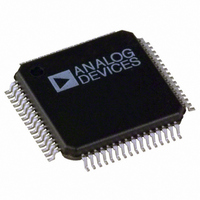
ADUC7128BSTZ126-RL Analog Devices Inc, ADUC7128BSTZ126-RL Datasheet - Page 67

ADUC7128BSTZ126-RL
Manufacturer Part Number
ADUC7128BSTZ126-RL
Description
IC DAS MCU ARM7 ADC/DDS 64-LQFP
Manufacturer
Analog Devices Inc
Series
MicroConverter® ADuC7xxxr
Datasheet
1.EVAL-ADUC7128QSPZ.pdf
(92 pages)
Specifications of ADUC7128BSTZ126-RL
Core Size
16/32-Bit
Program Memory Size
126KB (126K x 8)
Core Processor
ARM7
Speed
41.78MHz
Connectivity
I²C, SPI, UART/USART
Peripherals
PLA, POR, PWM, PSM, Temp Sensor, WDT
Number Of I /o
28
Program Memory Type
FLASH
Ram Size
8K x 8
Voltage - Supply (vcc/vdd)
3 V ~ 3.6 V
Data Converters
A/D 10x12b; D/A 1x10b
Oscillator Type
Internal
Operating Temperature
-40°C ~ 125°C
Package / Case
64-LQFP
Controller Family/series
(ARM7) ADUC
No. Of I/o's
40
Cpu Speed
41.78MHz
No. Of Timers
5
Digital Ic Case Style
LQFP
Embedded Interface Type
I2C, SPI, UART
Rohs Compliant
Yes
Lead Free Status / RoHS Status
Lead free / RoHS Compliant
For Use With
EVAL-ADUC7128QSPZ - KIT DEV FOR ADUC7128
Eeprom Size
-
Lead Free Status / RoHS Status
Lead free / RoHS Compliant, Lead free / RoHS Compliant
Other names
ADUC7128BSTZ126-RLTR
Available stocks
Company
Part Number
Manufacturer
Quantity
Price
Company:
Part Number:
ADUC7128BSTZ126-RL
Manufacturer:
Analog Devices Inc
Quantity:
10 000
I2CxSRX Register
Name
I2C0SRX
I2C1SRX
I2CxSRX is a receive register for the slave channel.
I2CxSTX Register
Name
I2C0STX
I2C1STX
I2CxSTX is a transmit register for the slave channel.
I2CxMRX Register
Name
I2CxMRX is a receive register for the master channel.
I2CxMTX Register
Name
I2C0MTX
I2C1MTX
I2CxMTX is a transmit register for the master channel.
I2CxCNT Register
Name
I2C0CNT
I2C1CNT
I2CxCNT is a master receive data count register. If a master read
transfer sequence is initiated, the I2CxCNT register denotes the
number of bytes (−1) to be read from the slave device. By default
this counter is 0, which corresponds to the expected one byte.
Table 94. I2C0CFG MMR Bit Designations
Bit
31:15
14
13
12
11
10
9
8
I2C0MRX
I2C1MRX
Description
Reserved. These bits should be written by the user as 0.
Enable Stop Interrupt.
Reserved. This bit should be written by the user as 0.
Reserved. This bit should be written by the user as 0.
Enable Stretch SCL. Holds SCL low.
Reserved. This bit should be written by the user as 0.
Slave Tx FIFO Request Interrupt Enable.
General Call Status Bit Clear.
Set by user to generate an interrupt upon receiving a stop condition and after receiving a valid start condition and matching
address.
Cleared by user to disable the generation of an interrupt upon receiving a stop condition.
Set by user to stretch the SCL line.
Cleared by user to disable stretching of the SCL line.
Cleared by user to generate an interrupt request just after the negative edge of the clock for the R/W bit. This allows the user to
input data into the slave Tx FIFO if it is empty. At 400 kSPS, and with the core clock running at 41.78 MHz, the user has 45 clock
cycles to take appropriate action, taking interrupt latency into account.
Set by user to disable the slave Tx FIFO request interrupt.
Set by user to clear the general call status bits.
Cleared automatically by hardware after the general call status bits have been cleared.
Address
0xFFFF0808
0xFFFF0908
Address
0xFFFF080C
0xFFFF090C
Address
Address
0xFFFF0814
0xFFFF0914
Address
0xFFFF0818
0xFFFF0918
0xFFFF0810
0xFFFF0910
Default Value
0x00
0x00
Default Value
0x00
0x00
Default Value
Default Value
0x00
0x00
Default Value
0x00
0x00
0x00
0x00
Access
R
R
Access
W
W
Access
Access
W
W
Access
R/W
R/W
R
R
Rev. 0 | Page 67 of 92
I2CxADR Register
Name
I2C0ADR
I2C1ADR
I2CxADR is a master address byte register. The I2CxADR value
is the device address that the master wants to communicate
with. It is automatically transmitted at the start of a master
transfer sequence if there is no valid data in the I2CxMTX
register when the master enable bit is set.
I2CxBYT Register
Name
I2C0BYT
I2C1BYT
I2CxBYT is a broadcast byte register.
I2CxALT Register
Name
I2C0ALT
I2C1ALT
I2CxALT is a hardware general call ID register used in slave mode.
I2CxCFG Register
Name
I2C0CFG
I2C1CFG
I2CxCFG is a configuration register.
Address
0xFFFF081C
0xFFFF091C
Address
0xFFFF0824
0xFFFF0924
Address
0xFFFF0828
0xFFFF0928
Address
0xFFFF082C
0xFFFF092C
Default Value
0x00
0x00
Default Value
0x00
0x00
Default Value
0x00
0x00
Default Value
0x00
0x00
Access
R/W
R/W
Access
R/W
R/W
Access
R/W
R/W
Access
R/W
R/W


