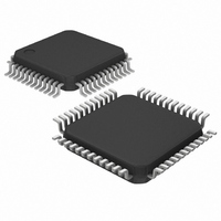
MAXQ7667AACM/V+ Maxim Integrated Products, MAXQ7667AACM/V+ Datasheet - Page 24

MAXQ7667AACM/V+
Manufacturer Part Number
MAXQ7667AACM/V+
Description
IC MCU-BASED DAS 16BIT 48-LQFP
Manufacturer
Maxim Integrated Products
Series
MAXQ™r
Datasheet
1.MAXQ7667AACMV.pdf
(40 pages)
Specifications of MAXQ7667AACM/V+
Core Processor
RISC
Core Size
16-Bit
Speed
16MHz
Connectivity
LIN, SPI, UART/USART
Peripherals
Brown-out Detect/Reset, POR, WDT
Number Of I /o
16
Program Memory Size
32KB (16K x 16)
Program Memory Type
FLASH
Ram Size
2K x 16
Voltage - Supply (vcc/vdd)
2.25 V ~ 2.75 V
Data Converters
A/D 5x12b
Oscillator Type
Internal
Operating Temperature
-40°C ~ 125°C
Package / Case
48-LQFP
Processor Series
MAXQ7667
Core
RISC
Data Bus Width
16 bit
Data Ram Size
4 KB
Interface Type
UART, JTAG, LIN
Maximum Clock Frequency
16 MHz
Number Of Programmable I/os
16
Number Of Timers
3
Operating Supply Voltage
5 V
Maximum Operating Temperature
+ 125 C
Mounting Style
SMD/SMT
Development Tools By Supplier
MAXQ7667EVKIT
Minimum Operating Temperature
- 40 C
On-chip Adc
12 bit, 5 Channel
Lead Free Status / RoHS Status
Lead free / RoHS Compliant
Eeprom Size
-
Lead Free Status / Rohs Status
Details
16-Bit, RISC, Microcontroller-Based,
Ultrasonic Distance-Measuring System
The following four digital I/Os form the TAP interface:
The MAXQ7667 includes a UART/LIN transceiver com-
bination that supports communication speeds up
2MBd. The LIN standard for example limits communica-
tion speed to 20kBd or less. Connect a LIN transceiver
or other UART connections such as RS-232 and RS-485
directly to the MAXQ7667’s 2-wire interface: URX and
UTX. The MAXQ7667 operates as a LIN slave or LIN
master device. The UART provides the programmable
baud-rate generators to communicate effectively to or
from the LIN transceiver. The device holds up to 8
bytes of data in each of the transmit and receive FIFOs.
The following characteristics apply to the MAXQ7667
UART/LIN interface:
24
• TDO—Serial output signal for test instruction and
• TDI—Serial input signal for test instruction and
• TCK—Serial clock for the test logic. When TCK
• TMS—Test mode selection. The rising edge of TCK
• Full-duplex operation for asynchronous data trans-
• Half-duplex operation for synchronous data trans-
• 8-deep receive and transmit FIFO with program-
• Independent baud-rate generator
• Programmable 9th data bit (commonly used for
• Hardware support for LIN including break detec-
data. Data transitions on the falling edge of TCK.
TDO idles high when inactive. TDO serially trans-
fers internal data to the external host. Data trans-
fers lease significant bit first.
data. Transition data on the rising edge of TCK.
TDO pulls high when unconnected. TDI serially
transfers data from the external host to the internal
TAP module shift registers. Data transfers least
significant bit first.
stops at 0, storage elements in the test logic must
retain their data indefinitely. Force TCK high when
inactive.
samples the test signals at TMS. The TAP controller
decodes the test signals at TMS to control the test
operation. Force TMS high when inactive.
fers up to 500kBd (system clock/32)
fers up to 2MBd (system clock/8)
mable interrupt for receive and transmit
parity or address/data selection)—UART mode
only
tion, autobaud, address identity filtering, check-
sum calculation, and block length checking
______________________________________________________________________________________
UART/LIN Interface
The MAXQ7667 supports 4-wire SPI interface communi-
cation with 8-bit or 16-bit data streams operating in
either master mode or slave mode. The SPI interface
allows synchronous half-duplex or full-duplex serial
data transfers to a wide variety of external serial
devices using MISO, MOSI, SS, and SCLK signals.
Collision detection is provided when two or more mas-
ters attempt a data transfer at the same time. See
Section 9 of the MAXQ7667 User’s Guide .
Two 8-bit digital I/O ports (P0._ and P1._), with dedicat-
ed one or more alternative functions, are available as
general-purpose I/Os (GPIOs) under the control of the
integrated MAXQ20. Set each I/O within each port indi-
vidually as an input or output. The GPIOs incorporate a
Schmitt trigger receiver and a full CMOS output driver
(Figure 13). Each GPIO configures as an input with
pullup to DVDDIO at power-up. When programmed as
an input, each I/O is configurable for high-impedance,
weak pullup to DVDDIO or pulldown to DGND. When
programmed as an output, writing to the port output
register (PO) controls the output logic state. The out-
puts source or sink at least 1.6mA. Configure the drive
strength for each I/O within each port to high or low
using the pad drive strength register for optimum EMI
performance. All the I/O ports have interrupt capability
that wake up the device while in stop mode and have
protection circuitry to DVDDIO and DGND.
The MAXQ7667 requires three different power-supply
voltages. DVDDIO, nominally +5V, allows interfacing to
standard 5V logic on all the digital I/Os including the
LIN/UART, JTAG, and SPI ports. DVDD, nominally
+2.5V, powers all the high-speed digital circuits. AVDD,
nominally 3.3V, powers the analog circuits.
External power supplies or internal voltage regulators
provide each of the supply voltages. The internal volt-
age regulators provide 3.3V and 2.5V supplies from the
5V DVDDIO input. Obtain the 5V supply from a higher
external voltage supply by using a few external compo-
nents. The MAXQ7667 includes an internal error ampli-
fier used to regulate the voltage on DVDDIO by driving
the gate or base of an external pass transistor. Refer to
the MAXQ7667 User’s Guide for more details on the
external components needed for 5V regulation.
• Supports common RS-232 and LIN baud rates:
1000, 1200, 2400, 4800, 9600, 19,200, 20,000,
38,400, 57,600, and 115,200 with system clock =
16MHz.
General-Purpose Digital I/O Ports
Supply-Voltage Regulators
SPI Interface


