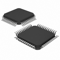
MAXQ7667AACM/V+ Maxim Integrated Products, MAXQ7667AACM/V+ Datasheet - Page 27

MAXQ7667AACM/V+
Manufacturer Part Number
MAXQ7667AACM/V+
Description
IC MCU-BASED DAS 16BIT 48-LQFP
Manufacturer
Maxim Integrated Products
Series
MAXQ™r
Datasheet
1.MAXQ7667AACMV.pdf
(40 pages)
Specifications of MAXQ7667AACM/V+
Core Processor
RISC
Core Size
16-Bit
Speed
16MHz
Connectivity
LIN, SPI, UART/USART
Peripherals
Brown-out Detect/Reset, POR, WDT
Number Of I /o
16
Program Memory Size
32KB (16K x 16)
Program Memory Type
FLASH
Ram Size
2K x 16
Voltage - Supply (vcc/vdd)
2.25 V ~ 2.75 V
Data Converters
A/D 5x12b
Oscillator Type
Internal
Operating Temperature
-40°C ~ 125°C
Package / Case
48-LQFP
Processor Series
MAXQ7667
Core
RISC
Data Bus Width
16 bit
Data Ram Size
4 KB
Interface Type
UART, JTAG, LIN
Maximum Clock Frequency
16 MHz
Number Of Programmable I/os
16
Number Of Timers
3
Operating Supply Voltage
5 V
Maximum Operating Temperature
+ 125 C
Mounting Style
SMD/SMT
Development Tools By Supplier
MAXQ7667EVKIT
Minimum Operating Temperature
- 40 C
On-chip Adc
12 bit, 5 Channel
Lead Free Status / RoHS Status
Lead free / RoHS Compliant
Eeprom Size
-
Lead Free Status / Rohs Status
Details
not externally forced low. An internal POR flag indicates
the source of a reset. Ramp up the DVDD supply at a
minimum rate of 60mV/ms to keep the device in POR
until DVDD fully settles.
The primary function of the watchdog timer is to watch
for stalled or stuck software. The watchdog timer per-
forms a controlled system restart when the µP fails to
write to the watchdog timer register before a selectable
timeout interval expires. The internal 13.5MHz RC oscil-
lator drives the MAXQ7667’s watchdog timer.
Figure 14 shows the watchdog timer functions as the
source of both the watchdog interrupt and watchdog
reset. The watchdog interrupt timeout period is pro-
grammable to 2
oscillator resulting in a nominal range of 273µs to
139.8ms. The watchdog reset timeout period is a fixed
512 RC clock cycles (34µs). When enabled, the watch-
dog generates an interrupt upon expiration; then, if not
reset within 512 RC clock cycles, the watchdog asserts
RESET low for eight RC clock cycles.
A hardware multiplier supports high-speed multiplica-
tions. The multiplier completes a 16-bit x 16-bit multipli-
cation in a single clock cycle and contains a 48-bit
accumulator. The multiplier is a peripheral that per-
forms seven different multiplication operations:
Figure 14. Watchdog Functional Diagram
RC CLOCK
(13.5MHz)
• Unsigned 16-bit multiplication
• Unsigned 16-bit multiplication and accumulation
• Unsigned 16-bit multiplication and subtraction
WD1
WD0
RWT
DIV 2
Hardware Multiplier/Accumulator
12
12
2
12
______________________________________________________________________________________
, 2
2
15
TIME
Ultrasonic Distance-Measuring System
15
DIV 2
2
TIMEOUT
, 2
18
RESET
WDIF
3
2
18
21
, or 2
16-Bit, RISC, Microcontroller-Based,
EWDI
EWT
DIV 2
Watchdog Timer
21
3
cycles of the RC
DIV 2
3
INTERRUPT
WTRF
RESET
The MAXQ20 µC is an accumulator-based Harvard
memory architecture. Fetch and execution operations
complete in one clock cycle without pipelining because
the instruction contains both the op code and data. The
µC streamlines 16 million instructions per second
(MIPS). Integrated 16-level hardware stack enables fast
subroutine calling and task switching. Manipulate data
quickly and efficiently with three internal data pointers.
Multiple data pointers allow more than one function to
access data memory without having to save and
restore data pointers each time. The data pointers auto-
matically increment or decrement following an opera-
tion, eliminating the need for software intervention.
The instruction set consists of a total of 33 fixed-length
16-bit instructions that operate on registers and memo-
ry locations. The highly orthogonal instruction set allows
arithmetic and logical operations to use any register
along with the accumulator. System registers control
functionality common to all MAXQ µCs, while peripheral
registers control peripherals and functions specific to
the MAXQ7667. All registers are subdivided into regis-
ter modules.
The architecture is transport-triggered. Writes or reads
from certain register locations potentially have side
effects. These side effects form the basis for the higher
level op codes defined by the assembler, such as
ADDC, OR, JUMP, etc. The op codes are implemented
as MOVE instructions between system registers. The
assembler handles all the instruction encoding.
In addition to the internal register space, the device
incorporates several memory areas:
Use the internal memory-management unit (MMU) to
map data memory space into a predefined program
memory segment for code execution from data memory.
Use the MMU to map program memory space as data
space for access to constant data stored in program
• Signed 16-bit multiplication
• Signed 16-bit multiplication and negation
• Signed 16-bit multiplication and accumulation
• Signed 16-bit multiplication and subtraction
• 16Kwords of flash memory for program storage
• 2Kword of SRAM for storage of temporary variables
• 4Kwords utility ROM
• 16-level, 16-bit-wide hardware stack for storage of
program return addresses and general-purpose use
MAXQ Core Architecture
Memory Organization
Instruction Set
27


