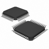
MAXQ7667AACM/V+ Maxim Integrated Products, MAXQ7667AACM/V+ Datasheet - Page 8

MAXQ7667AACM/V+
Manufacturer Part Number
MAXQ7667AACM/V+
Description
IC MCU-BASED DAS 16BIT 48-LQFP
Manufacturer
Maxim Integrated Products
Series
MAXQ™r
Datasheet
1.MAXQ7667AACMV.pdf
(40 pages)
Specifications of MAXQ7667AACM/V+
Core Processor
RISC
Core Size
16-Bit
Speed
16MHz
Connectivity
LIN, SPI, UART/USART
Peripherals
Brown-out Detect/Reset, POR, WDT
Number Of I /o
16
Program Memory Size
32KB (16K x 16)
Program Memory Type
FLASH
Ram Size
2K x 16
Voltage - Supply (vcc/vdd)
2.25 V ~ 2.75 V
Data Converters
A/D 5x12b
Oscillator Type
Internal
Operating Temperature
-40°C ~ 125°C
Package / Case
48-LQFP
Processor Series
MAXQ7667
Core
RISC
Data Bus Width
16 bit
Data Ram Size
4 KB
Interface Type
UART, JTAG, LIN
Maximum Clock Frequency
16 MHz
Number Of Programmable I/os
16
Number Of Timers
3
Operating Supply Voltage
5 V
Maximum Operating Temperature
+ 125 C
Mounting Style
SMD/SMT
Development Tools By Supplier
MAXQ7667EVKIT
Minimum Operating Temperature
- 40 C
On-chip Adc
12 bit, 5 Channel
Lead Free Status / RoHS Status
Lead free / RoHS Compliant
Eeprom Size
-
Lead Free Status / Rohs Status
Details
16-Bit, RISC, Microcontroller-Based,
Ultrasonic Distance-Measuring System
ELECTRICAL CHARACTERISTICS (continued)
(V
(f
otherwise specified. Typical values are at T
Note 1: Noise measured at bandpass filter output with ECHO+ and ECHO- shorted divided by the gain with f
Note 2: Gain adjust resolution typically ranges between 6.25% and 12.5%.
Note 3: LIN 2.0 specifies a maximim data rate of 20kbps. Higher data rates could be possible with compatible devices and suitable
8
BPF
SPI INTERFACE TIMING (Figures 11 and 12)
SPI Master Operating
Frequency
SPI Slave Operating
Frequency
SCLK Output Pulse-Width
High/Low
MOSI Output Hold Time
After SCLK Sample Edge
MOSI Output Valid to Sample
Edge
MISO Input Valid to SCLK
Sample Edge
MISO Input Hold Time After
SCLK Sample Edge
SCLK Inactive to MOSI
Inactive
SCLK Input Pulse-Width
High/Low
SS Active to First Shift Edge
MOSI Input Setup Time to
SCLK Sample Edge
MOSI Input Hold Time After
SCLK Sample Edge
MISO Output Valid After
SCLK Shift Edge Transition
SS Inactive Duration
SCLK Inactive to SS Rising
Edge
FLASH PROGRAMMING
Flash Erase Time
Flash Programming Time
Write/Erase Cycles
Data Retention
DVDDIO
_______________________________________________________________________________________
) = 50kHz, C
line conditions.
PARAMETER
= +5V, V
REFBG
AVDD
= C
= +3.3V; V
REF
= 1µF in parallel with 0.01µF, f
SYMBOL
1/t
1/t
t
t
t
t
t
t
MCH
t
t
t
DVDD
t
t
SCH
t
MOH
MOV
t
t
MCL
MLH
SOV
SSH
t
MIH
SCL
SSE
MIS
SIS
SIH
SD
MCK
SCK
,
,
= +2.5V, system clock (f
A
= +25°C.)
0.5 x f
0.25 x f
Mass erase
Page erase (512 bytes per page)
20µs per word
Average temperature = +85°C
SYSCLK
SYSCLK
CONDITIONS
ADCCLK
SYSCLK
= 2MHz (SAR data rate = 125ksps), T
) = 16MHz, burst frequency (f
t
t
4t
SYSCLK
SYSCLK
t
t
t
10,000
MCK
MCK
MCK
SYSCLK
MIN
- 25
- 25
- 25
200
657
25
25
25
25
25
20
15
0
0
/2
/2
/2
+
+
t
SCK
TYP
BURST
/2
A
) = bandpass frequency
BPF
= T
MAX
50
= 50kHz.
MIN
8
4
to T
MAX
UNITS
Cycles
Years
MHz
MHz
ms
ms
, unless
ns
ns
ns
ns
ns
ns
ns
ns
ns
ns
ns
ns
ns


