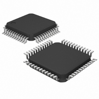
MAXQ7667AACM/V+ Maxim Integrated Products, MAXQ7667AACM/V+ Datasheet - Page 28

MAXQ7667AACM/V+
Manufacturer Part Number
MAXQ7667AACM/V+
Description
IC MCU-BASED DAS 16BIT 48-LQFP
Manufacturer
Maxim Integrated Products
Series
MAXQ™r
Datasheet
1.MAXQ7667AACMV.pdf
(40 pages)
Specifications of MAXQ7667AACM/V+
Core Processor
RISC
Core Size
16-Bit
Speed
16MHz
Connectivity
LIN, SPI, UART/USART
Peripherals
Brown-out Detect/Reset, POR, WDT
Number Of I /o
16
Program Memory Size
32KB (16K x 16)
Program Memory Type
FLASH
Ram Size
2K x 16
Voltage - Supply (vcc/vdd)
2.25 V ~ 2.75 V
Data Converters
A/D 5x12b
Oscillator Type
Internal
Operating Temperature
-40°C ~ 125°C
Package / Case
48-LQFP
Processor Series
MAXQ7667
Core
RISC
Data Bus Width
16 bit
Data Ram Size
4 KB
Interface Type
UART, JTAG, LIN
Maximum Clock Frequency
16 MHz
Number Of Programmable I/os
16
Number Of Timers
3
Operating Supply Voltage
5 V
Maximum Operating Temperature
+ 125 C
Mounting Style
SMD/SMT
Development Tools By Supplier
MAXQ7667EVKIT
Minimum Operating Temperature
- 40 C
On-chip Adc
12 bit, 5 Channel
Lead Free Status / RoHS Status
Lead free / RoHS Compliant
Eeprom Size
-
Lead Free Status / Rohs Status
Details
16-Bit, RISC, Microcontroller-Based,
Ultrasonic Distance-Measuring System
memory. Access physical memory segments (other
than the stack and register memories) as either pro-
gram memory or data memory, but not both at once.
By default, the memory is arranged in a Harvard archi-
tecture, with separate address spaces for program and
data memory. The configuration of program and data
space depends on the current execution location.
The utility ROM is a 4K x 16 block of internal ROM
memory that defaults to a starting address of 8000h.
The utility ROM consists of subroutines called from
application software. The subroutines include:
Following any reset, execution begins in the utility ROM.
The ROM software determines whether the program
execution immediately jumps to the start of the user-
application code (located at address 0000h) or to one
of the special routines mentioned above. Call the rou-
tines within the utility ROM using the application soft-
ware. Refer to the MAXQ7667 User’s Guide for more
information on the utility ROM contents.
Password protect in-system programming, in-applica-
tion programming, and in-circuit debugging functions
using a password-lock (PWL) bit. The PWL bit is imple-
mented in the SC register. When the PWL bit is set to
one (POR default), the password is required to access
the utility ROM, including in-circuit debug and in-sys-
tem programming routines that allow reading or writing
of internal memory. When the PWL bit is cleared to
zero, these utilities are fully accessible without the
password. The password is automatically set to all ones
following a mass erase.
28
• When executing code from flash memory, access
• When executing code from SRAM, access the
• When executing code from the utility ROM, access
• In-system programming (bootloader) over the
• In-circuit debug routines
• Test routines (internal memory tests, memory
• User-callable routines for in-application flash pro-
the SRAM and utility ROM in data space.
flash memory and utility ROM in data space.
the flash memory and SRAM in data space.
JTAG or UART interface
loader, etc.)
gramming and code space table lookup
______________________________________________________________________________________
Utility ROM (see Section 18 of
the MAXQ7667 User’s Guide)
The 2K x 16 internal data SRAM maps into either pro-
gram or data space. The contents of the SRAM are
maintained during stop mode and across non-POR
resets, as long as DVDD remains within the operating
voltage range.
A data memory cycle requires only one system clock
period to support fast internal execution. This allows a
complete read or write operation on SRAM in one clock
cycle. The MMU handles data memory mapping and
access control. Read or write to the data memory with
word or byte-wide commands.
The MAXQ7667 provides a 16 x 16 hardware stack to
support subroutine calls and system interrupts. A 16-bit
wide internal hardware stack provides storage for pro-
gram return addresses and general-purpose use. The
stack is used automatically by the processor when the
CALL, RET, and RETI instructions are executed and
interrupts serviced.
Sets of registers control most functions. These registers
provide a working space for memory operations as well
as configuring and addressing peripheral registers on
the device. Registers are divided into two major types;
system registers and peripheral registers. The register
set common to most MAXQ-based devices, also known
as the system registers, includes the ALU, accumulator
registers, data pointers, interrupt vectors and control,
and stack pointer. The peripheral registers define addi-
tional functionality. Tables 1 and 3 show the MAXQ7667
register set.
Two different methods program the flash memory: in-
system programming and in-application programming.
Both methods afford great flexibility in system design
as well as reduce the life-cycle cost of the embedded
system. The MAXQ7667 password protects these fea-
tures to prevent unauthorized access to code memory.
An internal bootstrap loader reloads the device over a
simple JTAG or UART interface allowing cost savings in
system software upgrade. During power-up, the
MAXQ7667 first checks for activity on the JTAG port. If
no activity is present, the device checks if a password-
protected program is present. If the password is set,
In-System Programming
Programming
Register Set
Stack Memory
Data Memory


