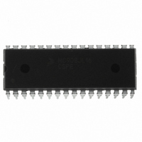
MC908JL16CSPE Freescale Semiconductor, MC908JL16CSPE Datasheet - Page 102

MC908JL16CSPE
Manufacturer Part Number
MC908JL16CSPE
Description
IC MCU 16K FLASH 8MHZ 32-SDIP
Manufacturer
Freescale Semiconductor
Series
HC08r
Datasheet
1.MC908JL16CFJER.pdf
(230 pages)
Specifications of MC908JL16CSPE
Core Processor
HC08
Core Size
8-Bit
Speed
8MHz
Connectivity
I²C, SCI
Peripherals
LED, LVD, POR, PWM
Number Of I /o
26
Program Memory Size
16KB (16K x 8)
Program Memory Type
FLASH
Ram Size
512 x 8
Voltage - Supply (vcc/vdd)
2.7 V ~ 5.5 V
Data Converters
A/D 13x10b
Oscillator Type
Internal
Operating Temperature
-40°C ~ 85°C
Package / Case
32-SDIP (0.400", 10.16mm)
Controller Family/series
HC08
No. Of I/o's
26
Ram Memory Size
512Byte
Cpu Speed
8MHz
No. Of Timers
2
Embedded Interface Type
I2C, SCI
Rohs Compliant
Yes
Processor Series
HC08JL
Core
HC08
Data Bus Width
8 bit
Data Ram Size
512 B
Interface Type
SCI
Maximum Clock Frequency
16 MHz
Number Of Programmable I/os
26
Number Of Timers
4
Operating Supply Voltage
2.7 V to 5.5 V
Maximum Operating Temperature
+ 85 C
Mounting Style
Through Hole
Development Tools By Supplier
FSICEBASE, DEMO908JL16E, M68CBL05CE
Minimum Operating Temperature
- 40 C
On-chip Adc
10 bit, 13 Channel
For Use With
DEMO908JL16E - BOARD DEMO FOR MC908JL16
Lead Free Status / RoHS Status
Lead free / RoHS Compliant
Eeprom Size
-
Lead Free Status / Rohs Status
Details
Available stocks
Company
Part Number
Manufacturer
Quantity
Price
Company:
Part Number:
MC908JL16CSPE
Manufacturer:
SONY
Quantity:
1 560
Part Number:
MC908JL16CSPE
Manufacturer:
FREESCALE
Quantity:
20 000
- Current page: 102 of 230
- Download datasheet (2Mb)
Serial Communications Interface (SCI)
7.8.3 SCI Control Register 3
SCI control register 3:
R8 — Received Bit 8
T8 — Transmitted Bit 8
DMARE — DMA Receive Enable Bit
DMATE — DMA Transfer Enable Bit
ORIE — Receiver Overrun Interrupt Enable Bit
102
•
•
•
When the SCI is receiving 9-bit characters, R8 is the read-only ninth bit (bit 8) of the received character.
R8 is received at the same time that the SCDR receives the other 8 bits. When the SCI is receiving
8-bit characters, R8 is a copy of the eighth bit (bit 7). Reset has no effect on the R8 bit.
When the SCI is transmitting 9-bit characters, T8 is the read/write ninth bit (bit 8) of the transmitted
character. T8 is loaded into the transmit shift register at the same time that the SCDR is loaded into
the transmit shift register. Reset has no effect on the T8 bit.
This read/write bit enables SCI error CPU interrupt requests generated by the receiver overrun bit, OR.
1 = DMA not enabled to service SCI receiver DMA service requests generated by the SCRF bit (SCI
0 = DMA not enabled to service SCI receiver DMA service requests generated by the SCRF bit (SCI
1 = SCTE DMA service requests enabled; SCTE CPU interrupt requests disabled
0 = SCTE DMA service requests disabled; SCTE CPU interrupt requests enabled
1 = SCI error CPU interrupt requests from OR bit enabled
0 = SCI error CPU interrupt requests from OR bit disabled
Stores the ninth SCI data bit received and the ninth SCI data bit to be transmitted
Enables these interrupts:
–
–
–
Parity error interrupts
Receiver overrun interrupts
Noise error interrupts
Framing error interrupts
receiver CPU interrupt requests enabled)
receiver CPU interrupt requests enabled)
Address:
The DMA module is not included on this MCU. Writing a logic 1 to DMARE
or DMATE may adversely affect MCU performance.
The DMA module is not included on this MCU. Writing a logic 1 to DMARE
or DMATE may adversely affect MCU performance.
Reset:
Read:
Write:
$0015
Bit 7
R8
U
Figure 7-11. SCI Control Register 3 (SCC3)
= Unimplemented
T8
U
6
MC68HC908JL16 Data Sheet, Rev. 1.1
DMARE
5
0
CAUTION
CAUTION
DMATE
4
0
U = Unaffected
ORIE
3
0
NEIE
2
0
FEIE
1
0
Freescale Semiconductor
PEIE
Bit 0
0
Related parts for MC908JL16CSPE
Image
Part Number
Description
Manufacturer
Datasheet
Request
R
Part Number:
Description:
Manufacturer:
Freescale Semiconductor, Inc
Datasheet:
Part Number:
Description:
Manufacturer:
Freescale Semiconductor, Inc
Datasheet:
Part Number:
Description:
Manufacturer:
Freescale Semiconductor, Inc
Datasheet:
Part Number:
Description:
Manufacturer:
Freescale Semiconductor, Inc
Datasheet:
Part Number:
Description:
Manufacturer:
Freescale Semiconductor, Inc
Datasheet:
Part Number:
Description:
Manufacturer:
Freescale Semiconductor, Inc
Datasheet:
Part Number:
Description:
Manufacturer:
Freescale Semiconductor, Inc
Datasheet:
Part Number:
Description:
Manufacturer:
Freescale Semiconductor, Inc
Datasheet:
Part Number:
Description:
Manufacturer:
Freescale Semiconductor, Inc
Datasheet:
Part Number:
Description:
Manufacturer:
Freescale Semiconductor, Inc
Datasheet:
Part Number:
Description:
Manufacturer:
Freescale Semiconductor, Inc
Datasheet:
Part Number:
Description:
Manufacturer:
Freescale Semiconductor, Inc
Datasheet:
Part Number:
Description:
Manufacturer:
Freescale Semiconductor, Inc
Datasheet:
Part Number:
Description:
Manufacturer:
Freescale Semiconductor, Inc
Datasheet:
Part Number:
Description:
Manufacturer:
Freescale Semiconductor, Inc
Datasheet:


