MC908JL16CSPE Freescale Semiconductor, MC908JL16CSPE Datasheet - Page 148
MC908JL16CSPE
Manufacturer Part Number
MC908JL16CSPE
Description
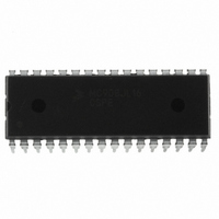
IC MCU 16K FLASH 8MHZ 32-SDIP
Manufacturer
Freescale Semiconductor
Series
HC08r
Datasheet
1.MC908JL16CFJER.pdf
(230 pages)
Specifications of MC908JL16CSPE
Core Processor
HC08
Core Size
8-Bit
Speed
8MHz
Connectivity
I²C, SCI
Peripherals
LED, LVD, POR, PWM
Number Of I /o
26
Program Memory Size
16KB (16K x 8)
Program Memory Type
FLASH
Ram Size
512 x 8
Voltage - Supply (vcc/vdd)
2.7 V ~ 5.5 V
Data Converters
A/D 13x10b
Oscillator Type
Internal
Operating Temperature
-40°C ~ 85°C
Package / Case
32-SDIP (0.400", 10.16mm)
Controller Family/series
HC08
No. Of I/o's
26
Ram Memory Size
512Byte
Cpu Speed
8MHz
No. Of Timers
2
Embedded Interface Type
I2C, SCI
Rohs Compliant
Yes
Processor Series
HC08JL
Core
HC08
Data Bus Width
8 bit
Data Ram Size
512 B
Interface Type
SCI
Maximum Clock Frequency
16 MHz
Number Of Programmable I/os
26
Number Of Timers
4
Operating Supply Voltage
2.7 V to 5.5 V
Maximum Operating Temperature
+ 85 C
Mounting Style
Through Hole
Development Tools By Supplier
FSICEBASE, DEMO908JL16E, M68CBL05CE
Minimum Operating Temperature
- 40 C
On-chip Adc
10 bit, 13 Channel
For Use With
DEMO908JL16E - BOARD DEMO FOR MC908JL16
Lead Free Status / RoHS Status
Lead free / RoHS Compliant
Eeprom Size
-
Lead Free Status / Rohs Status
Details
Available stocks
Company
Part Number
Manufacturer
Quantity
Price
Company:

Part Number:
MC908JL16CSPE
Manufacturer:
SONY
Quantity:
1 560
Part Number:
MC908JL16CSPE
Manufacturer:
FREESCALE
Quantity:
20 000


Input/Output (I/O) Ports
10.5.1 Port E Data Register (PTE)
The port E data register contains a data latch for each of the two port E pins.
PTE[1:0] — Port E Data Bits
T2CH1, T2CH0 — Timer 2 Channel I/Os
10.5.2 Data Direction Register E (DDRE)
Data direction register E determines whether each port E pin is an input or an output. Writing a logic 1 to
a DDRE bit enables the output buffer for the corresponding port E pin; a logic 0 disables the output buffer.
DDRE[1:0] — Data Direction Register E Bits
148
These read/write bits are software programmable. Data direction of each port E pin is under the control
of the corresponding bit in data direction register E. Reset has no effect on port D data.
The T2CH1 and T2CH0 pins are the TIM2 input capture/output compare pins. The edge/level select
bits, ELSxB:ELSxA, determine whether the PTE0/T2CH0 and PTE1/T2CH1 pins are timer channel I/O
pins or general-purpose I/O pins. See
These read/write bits control port E data direction. Reset clears DDRE[1:0], configuring all port E pins
as inputs.
1 = Corresponding port E pin configured as output
0 = Corresponding port E pin configured as input
Alternative Functions:
Address: $000C
Avoid glitches on port E pins by writing to the port E data register before
changing data direction register E bits from 0 to 1.
port E I/O logic.
Reset:
Read:
Write:
Address: $0008
Reset:
Read:
Write:
Bit 7
0
Figure 10-15. Data Direction Register E (DDRE)
Bit 7
= Unimplemented
Figure 10-14. Port E Data Register (PTE)
6
0
= Unimplemented
MC68HC908JL16 Data Sheet, Rev. 1.1
6
Chapter 6 Timer Interface Module
5
0
5
NOTE
4
0
Unaffected by reset
4
3
0
Figure 10-16
3
2
0
2
(TIM).
DDRE1
1
0
shows the
T2CH1
PTE1
1
Freescale Semiconductor
DDRE0
Bit 0
0
T2CH0
PTE0
Bit 0
Related parts for MC908JL16CSPE
Image
Part Number
Description
Manufacturer
Datasheet
Request
R

Part Number:
Description:
Manufacturer:
Freescale Semiconductor, Inc
Datasheet:
Part Number:
Description:
Manufacturer:
Freescale Semiconductor, Inc
Datasheet:
Part Number:
Description:
Manufacturer:
Freescale Semiconductor, Inc
Datasheet:
Part Number:
Description:
Manufacturer:
Freescale Semiconductor, Inc
Datasheet:
Part Number:
Description:
Manufacturer:
Freescale Semiconductor, Inc
Datasheet:
Part Number:
Description:
Manufacturer:
Freescale Semiconductor, Inc
Datasheet:
Part Number:
Description:
Manufacturer:
Freescale Semiconductor, Inc
Datasheet:
Part Number:
Description:
Manufacturer:
Freescale Semiconductor, Inc
Datasheet:
Part Number:
Description:
Manufacturer:
Freescale Semiconductor, Inc
Datasheet:
Part Number:
Description:
Manufacturer:
Freescale Semiconductor, Inc
Datasheet:
Part Number:
Description:
Manufacturer:
Freescale Semiconductor, Inc
Datasheet:
Part Number:
Description:
Manufacturer:
Freescale Semiconductor, Inc
Datasheet:
Part Number:
Description:
Manufacturer:
Freescale Semiconductor, Inc
Datasheet:
Part Number:
Description:
Manufacturer:
Freescale Semiconductor, Inc
Datasheet:
Part Number:
Description:
Manufacturer:
Freescale Semiconductor, Inc
Datasheet: