C8051F341-GQ Silicon Laboratories Inc, C8051F341-GQ Datasheet - Page 6
C8051F341-GQ
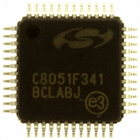
Manufacturer Part Number
C8051F341-GQ
Description
IC 8051 MCU FLASH 32K 48TQFP
Manufacturer
Silicon Laboratories Inc
Series
C8051F34xr
Datasheets
1.C8051F349-GQ.pdf
(276 pages)
2.C8051F341-GQ.pdf
(1 pages)
3.C8051F347-GQ.pdf
(296 pages)
Specifications of C8051F341-GQ
Program Memory Type
FLASH
Program Memory Size
32KB (32K x 8)
Package / Case
48-TQFP, 48-VQFP
Core Processor
8051
Core Size
8-Bit
Speed
48MHz
Connectivity
EBI/EMI, SMBus (2-Wire/I²C), SPI, UART/USART, USB
Peripherals
Brown-out Detect/Reset, POR, PWM, Temp Sensor, WDT
Number Of I /o
40
Ram Size
2.25K x 8
Voltage - Supply (vcc/vdd)
2.7 V ~ 3.6 V
Data Converters
A/D 20x10b
Oscillator Type
Internal
Operating Temperature
-40°C ~ 85°C
Processor Series
C8051F3x
Core
8051
Data Bus Width
8 bit
Data Ram Size
3.25 KB
Interface Type
I2C/SMBus/SPI/UART/USB
Maximum Clock Frequency
48 MHz
Number Of Programmable I/os
40
Number Of Timers
4
Operating Supply Voltage
2.7 V to 5.25 V
Maximum Operating Temperature
+ 85 C
Mounting Style
SMD/SMT
3rd Party Development Tools
KSK-SL-F34X, KSK-SL-TOOLSTICK, PK51, CA51, A51, ULINK2
Development Tools By Supplier
C8051F340DK
Minimum Operating Temperature
- 40 C
On-chip Adc
17-ch x 10-bit
No. Of I/o's
40
Ram Memory Size
2304Byte
Cpu Speed
48MHz
No. Of Timers
4
Rohs Compliant
Yes
Package
48TQFP
Device Core
8051
Family Name
C8051F34x
Maximum Speed
48 MHz
Data Rom Size
128 B
A/d Bit Size
10 bit
A/d Channels Available
17
Height
1 mm
Length
7 mm
Supply Voltage (max)
3.6 V
Supply Voltage (min)
2.7 V
Width
7 mm
Lead Free Status / RoHS Status
Lead free / RoHS Compliant
For Use With
336-1748 - ADAPTER TOOLSTICK FOR C8051F34X770-1006 - ISP 4PORT FOR SILABS C8051F MCU336-1452 - ADAPTER PROGRAM TOOLSTICK F340
Eeprom Size
-
Lead Free Status / Rohs Status
Lead free / RoHS Compliant
Other names
336-1299
Available stocks
Company
Part Number
Manufacturer
Quantity
Price
Company:

Part Number:
C8051F341-GQ
Manufacturer:
Silicon Laboratories Inc
Quantity:
10 000
Company:
Part Number:
C8051F341-GQR
Manufacturer:
Silicon Laboratories Inc
Quantity:
10 000


C8051F340/1/2/3/4/5/6/7/8/9
18. UART0.................................................................................................................... 223
19. UART1 (C8051F340/1/4/5/8 Only) ........................................................................ 231
20. Enhanced Serial Peripheral Interface (SPI0)...................................................... 241
21. Timers.................................................................................................................... 255
6
17.2.SMBus Configuration...................................................................................... 206
17.3.SMBus Operation ........................................................................................... 206
17.4.Using the SMBus............................................................................................ 208
17.5.SMBus Transfer Modes.................................................................................. 216
17.6.SMBus Status Decoding................................................................................. 220
18.1.Enhanced Baud Rate Generation................................................................... 224
18.2.Operational Modes ......................................................................................... 224
18.3.Multiprocessor Communications .................................................................... 226
19.1.Baud Rate Generator ..................................................................................... 232
19.2.Data Format.................................................................................................... 233
19.3.Configuration and Operation .......................................................................... 234
20.1.Signal Descriptions......................................................................................... 242
20.2.SPI0 Master Mode Operation ......................................................................... 243
20.3.SPI0 Slave Mode Operation ........................................................................... 245
20.4.SPI0 Interrupt Sources ................................................................................... 245
20.5.Serial Clock Timing......................................................................................... 246
20.6.SPI Special Function Registers ...................................................................... 248
21.1.Timer 0 and Timer 1 ....................................................................................... 255
17.3.1.Arbitration............................................................................................... 207
17.3.2.Clock Low Extension.............................................................................. 208
17.3.3.SCL Low Timeout................................................................................... 208
17.3.4.SCL High (SMBus Free) Timeout .......................................................... 208
17.4.1.SMBus Configuration Register............................................................... 210
17.4.2.SMB0CN Control Register ..................................................................... 213
17.4.3.Data Register ......................................................................................... 216
17.5.1.Master Transmitter Mode ....................................................................... 216
17.5.2.Master Receiver Mode ........................................................................... 218
17.5.3.Slave Receiver Mode ............................................................................. 219
17.5.4.Slave Transmitter Mode ......................................................................... 220
18.2.1.8-Bit UART ............................................................................................. 225
18.2.2.9-Bit UART ............................................................................................. 226
19.3.1.Data Transmission ................................................................................. 234
19.3.2.Data Reception ...................................................................................... 234
19.3.3.Multiprocessor Communications ............................................................ 235
20.1.1.Master Out, Slave In (MOSI).................................................................. 242
20.1.2.Master In, Slave Out (MISO).................................................................. 242
20.1.3.Serial Clock (SCK) ................................................................................. 242
20.1.4.Slave Select (NSS) ................................................................................ 242
21.1.1.Mode 0: 13-bit Counter/Timer ................................................................ 255
21.1.2.Mode 1: 16-bit Counter/Timer ................................................................ 256
21.1.3.Mode 2: 8-bit Counter/Timer with Auto-Reload...................................... 257
Rev. 1.1
Related parts for C8051F341-GQ
Image
Part Number
Description
Manufacturer
Datasheet
Request
R

Part Number:
Description:
SMD/C°/SINGLE-ENDED OUTPUT SILICON OSCILLATOR
Manufacturer:
Silicon Laboratories Inc
Part Number:
Description:
Manufacturer:
Silicon Laboratories Inc
Datasheet:
Part Number:
Description:
N/A N/A/SI4010 AES KEYFOB DEMO WITH LCD RX
Manufacturer:
Silicon Laboratories Inc
Datasheet:
Part Number:
Description:
N/A N/A/SI4010 SIMPLIFIED KEY FOB DEMO WITH LED RX
Manufacturer:
Silicon Laboratories Inc
Datasheet:
Part Number:
Description:
N/A/-40 TO 85 OC/EZLINK MODULE; F930/4432 HIGH BAND (REV E/B1)
Manufacturer:
Silicon Laboratories Inc
Part Number:
Description:
EZLink Module; F930/4432 Low Band (rev e/B1)
Manufacturer:
Silicon Laboratories Inc
Part Number:
Description:
I°/4460 10 DBM RADIO TEST CARD 434 MHZ
Manufacturer:
Silicon Laboratories Inc
Part Number:
Description:
I°/4461 14 DBM RADIO TEST CARD 868 MHZ
Manufacturer:
Silicon Laboratories Inc
Part Number:
Description:
I°/4463 20 DBM RFSWITCH RADIO TEST CARD 460 MHZ
Manufacturer:
Silicon Laboratories Inc
Part Number:
Description:
I°/4463 20 DBM RADIO TEST CARD 868 MHZ
Manufacturer:
Silicon Laboratories Inc
Part Number:
Description:
I°/4463 27 DBM RADIO TEST CARD 868 MHZ
Manufacturer:
Silicon Laboratories Inc
Part Number:
Description:
I°/4463 SKYWORKS 30 DBM RADIO TEST CARD 915 MHZ
Manufacturer:
Silicon Laboratories Inc
Part Number:
Description:
N/A N/A/-40 TO 85 OC/4463 RFMD 30 DBM RADIO TEST CARD 915 MHZ
Manufacturer:
Silicon Laboratories Inc
Part Number:
Description:
I°/4463 20 DBM RADIO TEST CARD 169 MHZ
Manufacturer:
Silicon Laboratories Inc