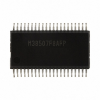
M38507F8AFP#U1 Renesas Electronics America, M38507F8AFP#U1 Datasheet - Page 37

M38507F8AFP#U1
Manufacturer Part Number
M38507F8AFP#U1
Description
IC 740/3850 MCU FLASH 42SSOP
Manufacturer
Renesas Electronics America
Series
740/38000r
Datasheet
1.M38507F8AFPU1.pdf
(61 pages)
Specifications of M38507F8AFP#U1
Core Processor
740
Core Size
8-Bit
Speed
12.5MHz
Connectivity
SIO, UART/USART
Peripherals
PWM, WDT
Number Of I /o
32
Program Memory Size
32KB (32K x 8)
Program Memory Type
FLASH
Ram Size
1K x 8
Voltage - Supply (vcc/vdd)
1.8 V ~ 5.5 V
Data Converters
A/D 9x10b
Oscillator Type
Internal
Operating Temperature
-20°C ~ 85°C
Package / Case
42-SSOP
Package
42SSOP
Family Name
740
Maximum Speed
12.5 MHz
Operating Supply Voltage
5 V
Data Bus Width
8 Bit
Number Of Programmable I/os
34
Interface Type
UART
On-chip Adc
9-chx10-bit
Number Of Timers
4
Lead Free Status / RoHS Status
Lead free / RoHS Compliant
Eeprom Size
-
Available stocks
Company
Part Number
Manufacturer
Quantity
Price
3850 Group (Spec.A QzROM version)
Rev.2.13
REJ03B0125-0213
WATCHDOG TIMER
The watchdog timer gives a mean of returning to the reset status
when a program cannot run on a normal loop (for example,
because of a software run-away). The watchdog timer consists of
an 8-bit watchdog timer L and an 8-bit watchdog timer H.
• Initial value of watchdog timer
At reset or writing to the watchdog timer control register
(address 0039
“FF
the instructions of STA, LDM, CLB and others can be used to
write. The data of bits 6 and 7 are only valid when writing to the
watchdog timer control register. Each of watchdog timer is set to
“FF
Bit 6 can be written to only once after reset release.
After this bit is written, it cannot rewritten because it is locked.
• Operation of Watchdog Timer
The watchdog timer stops at reset and starts to count down by
writing to the watchdog timer control register. An internal reset
occurs at an underflow of the watchdog timer H. The reset is
released after waiting for a reset release time and the program is
processed from the reset vector address. Accordingly,
programming is usually performed so that writing to the
watchdog timer control register may be started before an
underflow. If writing to the watchdog timer control register is not
performed once, the watchdog timer does not function.
Fig 37. Block diagram of Watchdog timer
Fig 38. Structure of Watchdog timer control register
Main clock division
ratio selection bits (Note)
16
16
X
” regardless of the written data of bits 0 to 5.
”. Any instruction which generates a write signal such as
X
CIN
IN
RESET
STP instruction function selection bit
Note: Any one of high-speed, middle-speed or low-speed mode is selected by bits 7 and 6 of the CPU mode register.
Apr 17, 2009
b7
16
), each of watchdog timer H and L is set to
“10”
“00”
“01”
STP instruction
Page 35 of 56
1/16
“FF
watchdog timer
control register is
written to.
16
” is set when
Watchdog timer L (8)
b0
Watchdog timer control register
(WDTCON : address 0039
Watchdog timer H (for read-out of high-order 6 bit)
STP instruction function selection bit
Watchdog timer H count source selection bit
0: Entering stop mode by execution of STP instruction
1: Internal reset by execution of STP instruction
0: Watchdog timer L underflow
1: f(X
IN
• Bit 6 of Watchdog Timer Control Register
• When bit 6 of the watchdog timer control register is “0”, the
• When bit 6 is “1”, execution of STP instruction causes an
The required time after writing to the watchdog timer control
register to an underflow of the watchdog timer H is shown as
follows.
When bit 7 of the watchdog timer control register is “0”:
When bit 7 of the watchdog timer control register is “1”:
Notes 1. The watchdog timer continues to count for waiting for a stop
)/16 or f(X
MCU enters the stop mode by execution of STP instruction.
Just after releasing the stop mode, the watchdog timer restarts
counting (Note). When executing the WIT instruction, the
watchdog timer does not stop.
internal reset. When this bit is set to “1” once, it cannot be
rewritten to “0” by program. Bit 6 is “0” at reset.
32 s at X
83.886ms at X
125 ms at X
327.68 µs at X
“0”
“1”
Watchdog timer H count
source selection bit
2. The watchdog timer cannot be used in the middle-speed mode.
mode release time. Do not generate an underflow of the watch-
dog timer H during that time.
(The internal reset may not be generated correctly, depending on
the underflow timing of the watchdog timer.)
CIN
CIN
CIN
)/16
= 32.768 kHz frequency and
IN
IN
16
Watchdog timer H (8)
= 32.768 kHz frequency and
)
= 12.5 MHz frequency.
= 12.5 MHz frequency.
Reset
circuit
Data bus
Internal reset
“FF
watchdog timer
control register is
written to.
16
” is set when


