M38507F8AFP#U1 Renesas Electronics America, M38507F8AFP#U1 Datasheet - Page 58
M38507F8AFP#U1
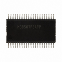
Manufacturer Part Number
M38507F8AFP#U1
Description
IC 740/3850 MCU FLASH 42SSOP
Manufacturer
Renesas Electronics America
Series
740/38000r
Datasheet
1.M38507F8AFPU1.pdf
(61 pages)
Specifications of M38507F8AFP#U1
Core Processor
740
Core Size
8-Bit
Speed
12.5MHz
Connectivity
SIO, UART/USART
Peripherals
PWM, WDT
Number Of I /o
32
Program Memory Size
32KB (32K x 8)
Program Memory Type
FLASH
Ram Size
1K x 8
Voltage - Supply (vcc/vdd)
1.8 V ~ 5.5 V
Data Converters
A/D 9x10b
Oscillator Type
Internal
Operating Temperature
-20°C ~ 85°C
Package / Case
42-SSOP
Package
42SSOP
Family Name
740
Maximum Speed
12.5 MHz
Operating Supply Voltage
5 V
Data Bus Width
8 Bit
Number Of Programmable I/os
34
Interface Type
UART
On-chip Adc
9-chx10-bit
Number Of Timers
4
Lead Free Status / RoHS Status
Lead free / RoHS Compliant
Eeprom Size
-
Available stocks
Company
Part Number
Manufacturer
Quantity
Price


3850 Group (Spec.A QzROM version)
Rev.2.13
REJ03B0125-0213
Handling of Source Pins
In order to avoid a latch-up occurrence, connect a capacitor
suitable for high frequencies as bypass capacitor between power
source pin (V
source pin (V
pin). Besides, connect the capacitor to as close as possible. For
bypass capacitor which should not be located too far from the
pins to be connected, a ceramic capacitor of 0.01
recommended.
Power Source Voltage
When the power source voltage value of a microcomputer is less
than the value which is indicated as the recommended operating
conditions, the microcomputer does not operate normally and
may perform unstable operation.
In a system where the power source voltage drops slowly when
the power source voltage drops or the power supply is turned off,
reset a microcomputer when the power source voltage is less
than the recommended operating conditions and design a system
not to cause errors to the system by this unstable operation.
Electric Characteristic Differences Between Flash
Memory, Mask ROM and QzROM Version MCUs
There are differences in the manufacturing processes and the
mask pattern among flash memory, mask ROM, and QzROM
version MCUs due to the differences of the ROM type. Even
when the ROM type is the same, when the memory size is
different, the manufacturing processes and the mask pattern
differ. For these reasons, the oscillation circuit constants and the
characteristics such as a characteristic value, operation margin,
noise immunity, and noise radiation within the limits of electrical
characteristics may differ.
When manufacturing an application system, please perform
sufficient evaluations in each product. Especially, when
switching a product (example: change from the mask ROM
version to QzROM version), please perform sufficient
evaluations by the switching product in the stage before mass-
producing an application system.
Product Shipped in Blank
As for the product shipped in blank, Renesas does not perform
the writing test to user ROM area after the assembly process
though the QzROM writing test is performed enough before the
assembly process. Therefore, a writing error of approx.0.1 %
may occur. Moreover, please note the contact of cables and
foreign bodies on a socket, etc. because a writing environment
may cause some writing errors.
QzROM Version
Connect the CNV
pattern which is supplied to the V
In addition connecting an approximately 5 kΩ resistor in series to
the GND could improve noise immunity. In this case as well as
the above mention, connect the pin the shortest possible to the
GND pattern which is supplied to the V
microcomputer.
• Reason
The CNV
QzROM. When programming in the QzROM, the impedance of
the V
into the built-in QzROM. Because of this, noise can enter easily.
If noise enters the V
are read from the QzROM, which may cause a program runaway.
PP
pin is low to allow the electric current for writing to flow
SS
/V
CC
CC
Apr 17, 2009
PP
pin) and GND pin (V
pin is the power source input pin for the built-in
pin) and analog power source input pin (AV
SS
/V
PP
PP
pin, abnormal instruction codes or data
pin the shortest possible to the GND
SS
Page 56 of 56
pin of the microcomputer.
SS
pin) and between power
S S
µ
F–0.1
pin of the
µ
F is
SS
Fig 55. Wiring for the CNV
Notes On QzROM Writing Orders
When ordering the QzROM product shipped after writing,
submit the mask file (extension: .mask) which is made by the
mask file converter MM.
• Be sure to set the ROM option data* setup when making the
• Set “FF
* ROM option data: mask option noted in MM
DATA REQUIRED FOR QzROM WRITING ORDERS
The following are necessary when ordering a QzROM product
shipped after writing:
1. QzROM Writing Confirmation Form*
2. Mark Specification Form*
3. ROM data...........Mask file
* For the QzROM writing confirmation form and the mark
specification form, refer to the “Renesas Technology Corp.”
Homepage (http://www.renesas.com/homepage.jsp).
Note that we cannot deal with special font marking (customer's
trademark etc.) in QzROM microcomputer.
mask file by using the mask file converter MM.. The ROM
code protect is specified according to the ROM option data* in
the mask file which is submitted at ordering. Note that the
mask file which has nothing at the ROM option data* or has
the data other than “00
regardless of the presence or absence of a protect. When data
other than “FF
submitted again.
16
Note. Shows the microcomputer’s pin.
” to the ROM code protect address in ROM data
CNV
16
” is set, we may ask that the ROM data be
SS
/V
V
16
PP
SS
” and “FF
(Note)
(Note)
SS
/V
16
PP
Approx. 5kΩ
” can not be accepted.
The shortest
The shortest
Related parts for M38507F8AFP#U1
Image
Part Number
Description
Manufacturer
Datasheet
Request
R

Part Number:
Description:
KIT STARTER FOR M16C/29
Manufacturer:
Renesas Electronics America
Datasheet:

Part Number:
Description:
KIT STARTER FOR R8C/2D
Manufacturer:
Renesas Electronics America
Datasheet:

Part Number:
Description:
R0K33062P STARTER KIT
Manufacturer:
Renesas Electronics America
Datasheet:

Part Number:
Description:
KIT STARTER FOR R8C/23 E8A
Manufacturer:
Renesas Electronics America
Datasheet:

Part Number:
Description:
KIT STARTER FOR R8C/25
Manufacturer:
Renesas Electronics America
Datasheet:

Part Number:
Description:
KIT STARTER H8S2456 SHARPE DSPLY
Manufacturer:
Renesas Electronics America
Datasheet:

Part Number:
Description:
KIT STARTER FOR R8C38C
Manufacturer:
Renesas Electronics America
Datasheet:

Part Number:
Description:
KIT STARTER FOR R8C35C
Manufacturer:
Renesas Electronics America
Datasheet:

Part Number:
Description:
KIT STARTER FOR R8CL3AC+LCD APPS
Manufacturer:
Renesas Electronics America
Datasheet:
Part Number:
Description:
KIT STARTER FOR RX610
Manufacturer:
Renesas Electronics America
Datasheet:

Part Number:
Description:
KIT STARTER FOR R32C/118
Manufacturer:
Renesas Electronics America
Datasheet:

Part Number:
Description:
KIT DEV RSK-R8C/26-29
Manufacturer:
Renesas Electronics America
Datasheet:

Part Number:
Description:
KIT STARTER FOR SH7124
Manufacturer:
Renesas Electronics America
Datasheet:

Part Number:
Description:
KIT STARTER FOR H8SX/1622
Manufacturer:
Renesas Electronics America
Datasheet:

Part Number:
Description:
KIT DEV FOR SH7203
Manufacturer:
Renesas Electronics America
Datasheet: