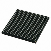
MCIMX515CJM6C Freescale Semiconductor, MCIMX515CJM6C Datasheet - Page 113

MCIMX515CJM6C
Manufacturer Part Number
MCIMX515CJM6C
Description
MULTIMEDIA PROC 529-LFBGA
Manufacturer
Freescale Semiconductor
Series
i.MX51r
Datasheets
1.MCIMX512DJM8C.pdf
(200 pages)
2.MCIMX515DJM8C.pdf
(2 pages)
3.MCIMX512CJM6C.pdf
(198 pages)
Specifications of MCIMX515CJM6C
Core Processor
ARM Cortex-A8
Core Size
32-Bit
Speed
600MHz
Connectivity
1-Wire, EBI/EMI, Ethernet, I²C, IrDA, MMC, SPI, SSI, UART/USART, USB OTG
Peripherals
DMA, I²S, LCD, POR, PWM, WDT
Number Of I /o
128
Program Memory Type
ROMless
Ram Size
128K x 8
Voltage - Supply (vcc/vdd)
0.8 V ~ 1.15 V
Oscillator Type
External
Operating Temperature
-20°C ~ 85°C
Package / Case
529-LFBGA
Processor Series
i.MX51
Core
ARM Cortex A8
Data Bus Width
32 bit
Program Memory Size
36 KB
Data Ram Size
128 KB
Interface Type
I2C, SPI, SSI, UART, USB
Maximum Clock Frequency
200 MHz
Number Of Timers
5
Operating Supply Voltage
0.8 V to 1.15 V
Maximum Operating Temperature
+ 95 C
Mounting Style
SMD/SMT
3rd Party Development Tools
MDK-ARM, RL-ARM, ULINK2
Development Tools By Supplier
MCIMX51EVKJ
Minimum Operating Temperature
- 40 C
Lead Free Status / RoHS Status
Lead free / RoHS Compliant
Eeprom Size
-
Program Memory Size
-
Data Converters
-
Lead Free Status / Rohs Status
Lead free / RoHS Compliant
Available stocks
Company
Part Number
Manufacturer
Quantity
Price
Company:
Part Number:
MCIMX515CJM6C
Manufacturer:
Freescale Semiconductor
Quantity:
10 000
Part Number:
MCIMX515CJM6C
Manufacturer:
FREESCALE
Quantity:
20 000
Company:
Part Number:
MCIMX515CJM6CR2
Manufacturer:
Freescale Semiconductor
Quantity:
10 000
Figure 69
lists the timing parameters.
4.7.10
This section describes the electrical information of the PWM.The PWM can be programmed to select one
of three clock signals as its source frequency. The selected clock signal is passed through a prescaler before
being input to the counter. The output is available at the pulse-width modulator output (PWMO) external
pin.
Freescale Semiconductor
One-Wire bus
(BATT_LINE)
OW7
OW8
OW9
One-Wire bus
(BATT_LINE)
ID
depicts Write 1 Sequence timing,
Pulse Width Modulator (PWM) Timing Parameters
Write /Read Low Time
Transmission Time Slot
Release Time
i.MX51 Applications Processors for Consumer and Industrial Products, Rev. 4
Parameter
OW7
OW7
Figure 69. Write 1 Sequence Timing Diagram
Figure 70. Read Sequence Timing Diagram
Table 88. WR1 /RD Timing Parameters
OW9
Figure 70
OW8
t
Symbol
RELEASE
OW8
t
t
LOW1
SLOT
depicts the Read Sequence timing, and
Min
60
15
1
Typ
117
—
5
Electrical Characteristics
Max
120
15
45
Table 88
Unit
µs
µs
µs
113


