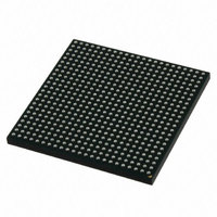
MCIMX515CJM6C Freescale Semiconductor, MCIMX515CJM6C Datasheet - Page 115

MCIMX515CJM6C
Manufacturer Part Number
MCIMX515CJM6C
Description
MULTIMEDIA PROC 529-LFBGA
Manufacturer
Freescale Semiconductor
Series
i.MX51r
Datasheets
1.MCIMX512DJM8C.pdf
(200 pages)
2.MCIMX515DJM8C.pdf
(2 pages)
3.MCIMX512CJM6C.pdf
(198 pages)
Specifications of MCIMX515CJM6C
Core Processor
ARM Cortex-A8
Core Size
32-Bit
Speed
600MHz
Connectivity
1-Wire, EBI/EMI, Ethernet, I²C, IrDA, MMC, SPI, SSI, UART/USART, USB OTG
Peripherals
DMA, I²S, LCD, POR, PWM, WDT
Number Of I /o
128
Program Memory Type
ROMless
Ram Size
128K x 8
Voltage - Supply (vcc/vdd)
0.8 V ~ 1.15 V
Oscillator Type
External
Operating Temperature
-20°C ~ 85°C
Package / Case
529-LFBGA
Processor Series
i.MX51
Core
ARM Cortex A8
Data Bus Width
32 bit
Program Memory Size
36 KB
Data Ram Size
128 KB
Interface Type
I2C, SPI, SSI, UART, USB
Maximum Clock Frequency
200 MHz
Number Of Timers
5
Operating Supply Voltage
0.8 V to 1.15 V
Maximum Operating Temperature
+ 95 C
Mounting Style
SMD/SMT
3rd Party Development Tools
MDK-ARM, RL-ARM, ULINK2
Development Tools By Supplier
MCIMX51EVKJ
Minimum Operating Temperature
- 40 C
Lead Free Status / RoHS Status
Lead free / RoHS Compliant
Eeprom Size
-
Program Memory Size
-
Data Converters
-
Lead Free Status / Rohs Status
Lead free / RoHS Compliant
Available stocks
Company
Part Number
Manufacturer
Quantity
Price
Company:
Part Number:
MCIMX515CJM6C
Manufacturer:
Freescale Semiconductor
Quantity:
10 000
Part Number:
MCIMX515CJM6C
Manufacturer:
FREESCALE
Quantity:
20 000
Company:
Part Number:
MCIMX515CJM6CR2
Manufacturer:
Freescale Semiconductor
Quantity:
10 000
Table 90
transfer modes.
The user needs to use level shifters for 5.0 V compatibility on the ATA interface. The i.MX51 P-ATA
interface is 3.3 V compatible.
The use of bus buffers introduces delay on the bus and introduces skew between signal lines. These factors
make it difficult to operate the bus at the highest speed (UDMA-4) when bus buffers are used. If fast
UDMA mode operation is needed, this may not be compatible with bus buffers.
Another area of attention is the slew rate limit imposed by the ATA specification on the ATA bus.
According to this limit, any signal driven on the bus should have a slew rate between 0.4 and 1.2 V/ns with
a 40 pF load. Not many vendors of bus buffers specify slew rate of the outgoing signals.
When bus buffers are used, the ata_data bus buffer is special. This is a bidirectional bus buffer, so a
direction control signal is needed. This direction control signal is ata_buffer_en. When its high, the bus
should drive from host to device. When its low, the bus should drive from device to host. Steering of the
signal is such that contention on the host and device tri-state busses is always avoided.
In the timing equations, some timing parameters are used. These parameters depend on the implementation
of the i.MX51 P-ATA interface on silicon, the bus buffer used, the cable delay and cable skew.
Freescale Semiconductor
1
SRISE and SFALL shall meet this requirement when measured at the sender’s connector from 10–90% of full signal
amplitude with all capacitive loads from 15
SI1
SI2
SI3
ID
ATA Interface Signals
and
Rising edge slew rate for any signal on ATA interface.
Falling edge slew rate for any signal on ATA interface (see note)
Host interface signal capacitance at the host connector
Figure 72
i.MX51 Applications Processors for Consumer and Industrial Products, Rev. 4
define the AC characteristics of all the P-ATA interface signals on all data
Table 90. AC Characteristics of All Interface Signals
Figure 72. P-ATA Interface Signals Timing Diagram
Parameter
–
40 pF where all signals have the same capacitive load value.
SI2
1
SI1
Symbol
C
S
S
host
rise
fall
Min
—
—
—
Electrical Characteristics
Max
1.25
1.25
20
Unit
V/ns
V/ns
pF
115


