AT89LP214-20XU Atmel, AT89LP214-20XU Datasheet - Page 2
AT89LP214-20XU
Manufacturer Part Number
AT89LP214-20XU
Description
MCU 8051 2K FLASH 20MHZ 14-TSSOP
Manufacturer
Atmel
Series
89LPr
Datasheet
1.AT89LP213-20PU.pdf
(98 pages)
Specifications of AT89LP214-20XU
Core Processor
8051
Core Size
8-Bit
Speed
20MHz
Connectivity
SPI, UART/USART
Peripherals
Brown-out Detect/Reset, POR, PWM, WDT
Number Of I /o
12
Program Memory Size
2KB (2K x 8)
Program Memory Type
FLASH
Ram Size
128 x 8
Voltage - Supply (vcc/vdd)
2.4 V ~ 5.5 V
Oscillator Type
Internal
Operating Temperature
-40°C ~ 85°C
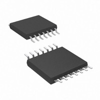
Package / Case
14-TSSOP
Package
14TSSOP
Device Core
8051
Family Name
AT89
Maximum Speed
20 MHz
Operating Supply Voltage
2.5|3.3|5 V
Data Bus Width
8 Bit
Number Of Programmable I/os
12
Interface Type
SPI/UART
Number Of Timers
2
Core
8051
Processor Series
AT89x
Maximum Clock Frequency
20 MHz
Data Ram Size
128 B
Mounting Style
SMD/SMT
Height
1.05 mm
Length
5.1 mm
Maximum Operating Temperature
+ 85 C
Minimum Operating Temperature
- 40 C
Supply Voltage (max)
5.5 V
Supply Voltage (min)
2.4 V
Width
4.5 mm
Lead Free Status / RoHS Status
Lead free / RoHS Compliant
Eeprom Size
-
Data Converters
-
Lead Free Status / Rohs Status
Details


2. Pin Configuration
2.1
2.2
2
AT89LP213: 14-lead TSSOP/PDIP
AT89LP214: 14-lead TSSOP/PDIP
AT89LP213/214
need only 1 to 4 clock cycles providing 6 to 12 times more throughput than the standard 8051.
Seventy percent of instructions need only as many clock cycles as they have bytes to execute,
and most of the remaining instructions require only one additional clock. The enhanced CPU
core is capable of 20 MIPS throughput whereas the classic 8051 CPU can deliver only 4 MIPS
at the same current consumption. Conversely, at the same throughput as the classic 8051, the
new CPU core runs at a much lower speed and thereby greatly reduces power consumption.
The AT89LP213/214 provides the following standard features: 2K bytes of In-System Program-
mable Flash memory, 128 bytes of RAM, up to 12 I/O lines, two 16-bit timer/counters, two PWM
outputs (AT89LP213 only), a programmable watchdog timer, a full duplex serial port
(AT89LP214 only), a serial peripheral interface, an internal 8 MHz RC oscillator, on-chip crystal
oscillator, and a four-level, six-vector interrupt system.
The two timer/counters in the AT89LP213/214 are enhanced with two new modes. Mode 0 can
be configured as a variable 9- to 16-bit timer/counter and Mode 1 can be configured as a 16-bit
auto-reload timer/counter. In addition, the timer/counters on the AT89LP213 may independently
drive a pulse width modulation output.
The I/O ports of the AT89LP213/214 can be independently configured in one of four operating
modes. In quasi-bidirectional mode, the ports operate as in the classic 8051. In input mode, the
ports are tristated. Push-pull output mode provides full CMOS drivers and open-drain mode pro-
vides just a pull-down. In addition, all 8 pins of Port 1 can be configured to generate an interrupt
using the general-purpose interrupt interface. The I/O pins of the AT89LP213/214 tolerate volt-
ages higher than the device’s own power supply, up to 5.5V. When the device is supplied at
2.4V and all I/O ports receive 5.5V, the total back flowing current in all I/Os is less than 100 µA.
(INT0/XTAL1) P3.2
(INT0/XTAL1) P3.2
(GPI5/MOSI) P1.5
(GPI5/MOSI) P1.5
(GPI7/SCK) P1.7
(GPI7/SCK) P1.7
(GPI5/RST) P1.3
(GPI5/RST) P1.3
(GPI2) P1.2
(GPI2) P1.2
(RxD) P3.0
(T0) P3.4
GND
GND
1
2
3
4
5
6
7
1
2
3
4
5
6
7
14
13
12
11
10
14
13
12
11
10
9
8
9
8
P1.6 (MISO/GPI6)
P1.4 (SS/GPI4)
P1.1 (AIN1/GPI1)
P1.0 (AIN0/GPI0)
VCC
P3.5 (T1)
P3.3 (XTAL2/CLKOUT/INT1)
P1.6 (MISO/GPI6)
P1.4 (SS/GPI4)
P1.1 (AIN1/GPI1)
P1.0 (AIN0/GPI0)
VCC
P3.1 (TxD)
P3.3 (XTAL2/CLKOUT/INT1)
3538E–MICRO–11/10
Related parts for AT89LP214-20XU
Image
Part Number
Description
Manufacturer
Datasheet
Request
R

Part Number:
Description:
Manufacturer:
Atmel Corporation
Datasheet:

Part Number:
Description:
MCU 8051 2K FLASH 20MHZ 14-PDIP
Manufacturer:
Atmel
Datasheet:

Part Number:
Description:
Microcontrollers (MCU) SINGLE CYCLE 2K ISP FLASH 2.4-5.5V
Manufacturer:
Atmel
Part Number:
Description:
At89lp213 8-bit Microcontroller With 2k Bytes Flash
Manufacturer:
ATMEL Corporation
Datasheet:

Part Number:
Description:
8-bit Microcontrollers - MCU Microcontroller
Manufacturer:
Atmel

Part Number:
Description:
DEV KIT FOR AVR/AVR32
Manufacturer:
Atmel
Datasheet:
Part Number:
Description:
INTERVAL AND WIPE/WASH WIPER CONTROL IC WITH DELAY
Manufacturer:
ATMEL Corporation
Datasheet:
Part Number:
Description:
Low-Voltage Voice-Switched IC for Hands-Free Operation
Manufacturer:
ATMEL Corporation
Datasheet:
Part Number:
Description:
MONOLITHIC INTEGRATED FEATUREPHONE CIRCUIT
Manufacturer:
ATMEL Corporation
Datasheet:
Part Number:
Description:
AM-FM Receiver IC U4255BM-M
Manufacturer:
ATMEL Corporation
Datasheet:
Part Number:
Description:
Monolithic Integrated Feature Phone Circuit
Manufacturer:
ATMEL Corporation
Datasheet:
Part Number:
Description:
Multistandard Video-IF and Quasi Parallel Sound Processing
Manufacturer:
ATMEL Corporation
Datasheet: