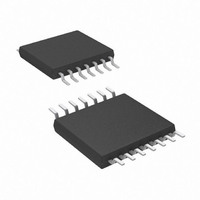
AT89LP214-20XU Atmel, AT89LP214-20XU Datasheet - Page 67

AT89LP214-20XU
Manufacturer Part Number
AT89LP214-20XU
Description
MCU 8051 2K FLASH 20MHZ 14-TSSOP
Manufacturer
Atmel
Series
89LPr
Datasheet
1.AT89LP213-20PU.pdf
(98 pages)
Specifications of AT89LP214-20XU
Core Processor
8051
Core Size
8-Bit
Speed
20MHz
Connectivity
SPI, UART/USART
Peripherals
Brown-out Detect/Reset, POR, PWM, WDT
Number Of I /o
12
Program Memory Size
2KB (2K x 8)
Program Memory Type
FLASH
Ram Size
128 x 8
Voltage - Supply (vcc/vdd)
2.4 V ~ 5.5 V
Oscillator Type
Internal
Operating Temperature
-40°C ~ 85°C
Package / Case
14-TSSOP
Package
14TSSOP
Device Core
8051
Family Name
AT89
Maximum Speed
20 MHz
Operating Supply Voltage
2.5|3.3|5 V
Data Bus Width
8 Bit
Number Of Programmable I/os
12
Interface Type
SPI/UART
Number Of Timers
2
Core
8051
Processor Series
AT89x
Maximum Clock Frequency
20 MHz
Data Ram Size
128 B
Mounting Style
SMD/SMT
Height
1.05 mm
Length
5.1 mm
Maximum Operating Temperature
+ 85 C
Minimum Operating Temperature
- 40 C
Supply Voltage (max)
5.5 V
Supply Voltage (min)
2.4 V
Width
4.5 mm
Lead Free Status / RoHS Status
Lead free / RoHS Compliant
Eeprom Size
-
Data Converters
-
Lead Free Status / Rohs Status
Details
23.2
3538E–MICRO–11/10
Memory Organization
The AT89LP213/214 offers 2K bytes of In-System Programmable (ISP) nonvolatile Flash code
memory. In addition, the device contains a 64-byte User Signature Array and a 32-byte read-
only Atmel Signature Array. The memory organization is shown in
The memory is divided into pages of 32 bytes each. A single read or write command may only
access a single page in the memory. Each memory type resides in its own address space and is
accessed by commands specific to that memory. However, all memory types share the same
page size.
User configuration fuses are mapped as a row in the memory, with each byte representing one
fuse. From a programming standpoint, fuses are treated the same as normal code bytes except
they are not affected by Chip Erase. Fuses can be enabled at any time by writing 00h to the
appropriate locations in the fuse row. However, to disable a fuse, i.e. set it to FFh, the entire
fuse row must be erased and then reprogrammed. The programmer should read the state of all
the fuses into a temporary location, modify those fuses which need to be disabled, then issue a
Fuse Write with Auto-Erase command using the temporary data. Lock bits are treated in a simi-
lar manner to fuses except they may only be erased (unlocked) by Chip Erase.
Table 23-1.
Figure 23-2. AT89LP213/214 Memory Organization
• The SS pin should not be left floating during reset if ISP is enabled.
• The ISP Enable Fuse must be set to allow programming during any reset period. If the ISP
driven low prior to the end of Power-On Reset (POR). After POR has completed the device
will remain in ISP mode until RST is brought high. Once the initial ISP session has ended, the
power to the target device must be cycled OFF and ON to enter another session.
Fuse is disabled, ISP may only be entered at POR.
AT89LP213
AT89LP214
Device #
Code Memory Sizes
Code Size
2K bytes
2K bytes
Atmel Signature Array
User Signature Array
Code Memory
User Fuse Row
Page Size
32 bytes
32 bytes
00
Page 63
Page 62
Page 0
Page 1
Page 0
Page 0
Page 1
Page 0
# Pages
64
64
AT89LP213/214
1F
Table 23-1
07FF
0000
Address Range
0000H - 07FFH
0000H - 07FFH
and
Figure
23-2.
67


