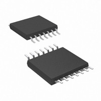
AT89LP214-20XU Atmel, AT89LP214-20XU Datasheet - Page 51

AT89LP214-20XU
Manufacturer Part Number
AT89LP214-20XU
Description
MCU 8051 2K FLASH 20MHZ 14-TSSOP
Manufacturer
Atmel
Series
89LPr
Datasheet
1.AT89LP213-20PU.pdf
(98 pages)
Specifications of AT89LP214-20XU
Core Processor
8051
Core Size
8-Bit
Speed
20MHz
Connectivity
SPI, UART/USART
Peripherals
Brown-out Detect/Reset, POR, PWM, WDT
Number Of I /o
12
Program Memory Size
2KB (2K x 8)
Program Memory Type
FLASH
Ram Size
128 x 8
Voltage - Supply (vcc/vdd)
2.4 V ~ 5.5 V
Oscillator Type
Internal
Operating Temperature
-40°C ~ 85°C
Package / Case
14-TSSOP
Package
14TSSOP
Device Core
8051
Family Name
AT89
Maximum Speed
20 MHz
Operating Supply Voltage
2.5|3.3|5 V
Data Bus Width
8 Bit
Number Of Programmable I/os
12
Interface Type
SPI/UART
Number Of Timers
2
Core
8051
Processor Series
AT89x
Maximum Clock Frequency
20 MHz
Data Ram Size
128 B
Mounting Style
SMD/SMT
Height
1.05 mm
Length
5.1 mm
Maximum Operating Temperature
+ 85 C
Minimum Operating Temperature
- 40 C
Supply Voltage (max)
5.5 V
Supply Voltage (min)
2.4 V
Width
4.5 mm
Lead Free Status / RoHS Status
Lead free / RoHS Compliant
Eeprom Size
-
Data Converters
-
Lead Free Status / Rohs Status
Details
3538E–MICRO–11/10
The interconnection between master and slave CPUs with SPI is shown in
pins in the interface are Master-In/Slave-Out (MISO), Master-Out/Slave-In (MOSI), Shift Clock
(SCK), and Slave Select (SS). The SCK pin is the clock output in master mode, but is the clock
input in slave mode. The MSTR bit in SPCR determines the directions of MISO and MOSI. Also
notice that MOSI connects to MOSI and MISO to MISO. In master mode, SS/P1.4 is ignored and
may be used as a general-purpose input or output. In slave mode, SS must be driven low to
select an individual device as a slave. When SS is driven high, the slave’s SPI port is deacti-
vated and the MOSI/P1.5 pin can be used as a general-purpose input.
Figure 18-1. SPI Master-slave Interconnection
The SPI has two modes of operation: normal (non-buffered write) and enhanced (buffered
write). In normal mode, writing to the SPI data register (SPDR) of the master CPU starts the SPI
clock generator and the data written shifts out of the MOSI pin and into the MOSI pin of the slave
CPU. Transmission may start after an initial delay while the clock generator waits for the next full
bit slot of the specified baud rate. After shifting one byte, the SPI clock generator stops, setting
the end of transmission flag (SPIF) and transferring the received byte to the read buffer (SPDR).
If both the SPI interrupt enable bit (SPIE) and the serial port interrupt enable bit (ES) are set, an
interrupt is requested. Note that SPDR refers to either the write data buffer or the read data buf-
fer, depending on whether the access is a write or read. In normal mode, because the write
buffer is transparent (and a write access to SPDR will be directed to the shift buffer), any attempt
to write to SPDR while a transmission is in progress will result in a write collision with WCOL set.
However, the transmission will still complete normally, but the new byte will be ignored and a
new write access to SPDR will be necessary.
Enhanced mode is similar to normal mode except that the write buffer holds the next byte to be
transmitted. Writing to SPDR loads the write buffer and sets WCOL to signify that the buffer is
full and any further writes will overwrite the buffer. WCOL is cleared by hardware when the
buffered byte is loaded into the shift register and transmission begins. If the master SPI is
currently idle, i.e. if this is the first byte, then after loading SPDR, transmission of the byte starts
and WCOL is cleared immediately. While this byte is transmitting, the next byte may be written
to SPDR. The Load Enable flag (LDEN) in SPSR can be used to determine when transmission
has started. LDEN is asserted during the first four bit slots of a SPI transfer. The master CPU
should first check that LDEN is set and that WCOL is cleared before loading the next byte. In
enhanced mode, if WCOL is set when a transfer completes, i.e. the next byte is available, then
the SPI immediately loads the buffered byte into the shift register, resets WCOL, and continues
transmission without stopping and restarting the clock generator. As long as the CPU can keep
the write buffer full in this manner, multiple bytes may be transferred with minimal latency
between bytes.
MSB
Generator
Clock
8-Bit Shift Register
Master
LSB
GPIO
GPIO
MISO
MOSI
SS
SCK
MISO
MOSI
SCK
SS
SSIG
MSB
DISSO
8-Bit Shift Register
AT89LP213/214
Slave
Figure
LSB
18-1. The four
51


