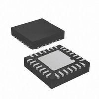
ATMEGA48V-10MMU Atmel, ATMEGA48V-10MMU Datasheet - Page 152

ATMEGA48V-10MMU
Manufacturer Part Number
ATMEGA48V-10MMU
Description
MCU AVR 4K FLASH 10MHZ 28-QFN
Manufacturer
Atmel
Series
AVR® ATmegar
Specifications of ATMEGA48V-10MMU
Core Processor
AVR
Core Size
8-Bit
Speed
10MHz
Connectivity
I²C, SPI, UART/USART
Peripherals
Brown-out Detect/Reset, POR, PWM, WDT
Number Of I /o
23
Program Memory Size
4KB (2K x 16)
Program Memory Type
FLASH
Eeprom Size
256 x 8
Ram Size
512 x 8
Voltage - Supply (vcc/vdd)
1.8 V ~ 5.5 V
Data Converters
A/D 8x10b
Oscillator Type
Internal
Operating Temperature
-40°C ~ 85°C
Package / Case
28-VQFN Exposed Pad, 28-HVQFN, 28-SQFN, 28-DHVQFN
Processor Series
ATMEGA48x
Core
AVR8
Data Bus Width
8 bit
Data Ram Size
512 B
Interface Type
2-Wire, SPI, USART, Serial
Maximum Clock Frequency
10 MHz
Number Of Programmable I/os
23
Number Of Timers
3
Maximum Operating Temperature
+ 85 C
Mounting Style
SMD/SMT
3rd Party Development Tools
EWAVR, EWAVR-BL
Minimum Operating Temperature
- 40 C
On-chip Adc
10 bit, 8 Channel
Package
28MLF EP
Device Core
AVR
Family Name
ATmega
Maximum Speed
10 MHz
Operating Supply Voltage
2.5|3.3|5 V
For Use With
ATSTK600 - DEV KIT FOR AVR/AVR32ATAVRDRAGON - KIT DRAGON 32KB FLASH MEM AVR
Lead Free Status / RoHS Status
Lead free / RoHS Compliant
Available stocks
Company
Part Number
Manufacturer
Quantity
Price
Company:
Part Number:
ATMEGA48V-10MMU
Manufacturer:
ZILOG
Quantity:
1
- Current page: 152 of 378
- Download datasheet (8Mb)
17.11 Register Description
17.11.1
152
ATmega48/88/168
TCCR2A – Timer/Counter Control Register A
The clock source for Timer/Counter2 is named clk
system I/O clock clk
clocked from the TOSC1 pin. This enables use of Timer/Counter2 as a Real Time Counter
(RTC). When AS2 is set, pins TOSC1 and TOSC2 are disconnected from Port C. A crystal can
then be connected between the TOSC1 and TOSC2 pins to serve as an independent clock
source for Timer/Counter2. The Oscillator is optimized for use with a 32.768 kHz crystal.
For Timer/Counter2, the possible prescaled selections are: clk
clk
Setting the PSRASY bit in GTCCR resets the prescaler. This allows the user to operate with a
predictable prescaler.
• Bits 7:6 – COM2A1:0: Compare Match Output A Mode
These bits control the Output Compare pin (OC2A) behavior. If one or both of the COM2A1:0
bits are set, the OC2A output overrides the normal port functionality of the I/O pin it is connected
to. However, note that the Data Direction Register (DDR) bit corresponding to the OC2A pin
must be set in order to enable the output driver.
When OC2A is connected to the pin, the function of the COM2A1:0 bits depends on the
WGM22:0 bit setting.
are set to a normal or CTC mode (non-PWM).
Table 17-2.
Table 17-3 on page 153
to fast PWM mode.
Bit
(0xB0)
Read/Write
Initial Value
T2S
COM2A1
/128, clk
0
0
1
1
T2S
Compare Output Mode, non-PWM Mode
COM2A1
R/W
/256, and clk
COM2A0
7
0
0
1
0
1
IO
Table 17-2
. By setting the AS2 bit in ASSR, Timer/Counter2 is asynchronously
COM2A0
shows the COM2A1:0 bit functionality when the WGM21:0 bits are set
R/W
6
0
Description
Normal port operation, OC2A disconnected.
Toggle OC2A on Compare Match
Clear OC2A on Compare Match
Set OC2A on Compare Match
T2S
/1024. Additionally, clk
shows the COM2A1:0 bit functionality when the WGM22:0 bits
COM2B1
R/W
5
0
COM2B0
R/W
4
0
T2S
. clk
R
3
–
0
T2S
T2S
as well as 0 (stop) may be selected.
is by default connected to the main
R
2
0
–
T2S
WGM21
/8, clk
R/W
1
0
T2S
WGM20
R/W
/32, clk
0
0
2545S–AVR–07/10
TCCR2A
T2S
/64,
Related parts for ATMEGA48V-10MMU
Image
Part Number
Description
Manufacturer
Datasheet
Request
R

Part Number:
Description:
IC AVR MCU 4K 5V 10MHZ 32-TQFP
Manufacturer:
Atmel
Datasheet:

Part Number:
Description:
IC AVR MCU 4K 10MHZ 1.8V 32-QFN
Manufacturer:
Atmel
Datasheet:

Part Number:
Description:
IC AVR MCU 4K 10MHZ 1.8V 28DIP
Manufacturer:
Atmel
Datasheet:

Part Number:
Description:
IC AVR MCU 4K 5V 10MHZ 32-TQFP
Manufacturer:
Atmel
Datasheet:

Part Number:
Description:
IC AVR MCU 4K 5V 12MHZ 32-QFN
Manufacturer:
Atmel
Datasheet:

Part Number:
Description:
IC AVR MCU 4K 5V 10MHZ 32-QFN
Manufacturer:
Atmel
Datasheet:

Part Number:
Description:
IC AVR MCU 4K 5V 10MHZ 28-DIP
Manufacturer:
Atmel
Datasheet:

Part Number:
Description:
IC AVR MCU 4K 5V 10MHZ 28-DIP
Manufacturer:
Atmel
Datasheet:

Part Number:
Description:
MCU AVR 4KB FLASH 10MHZ 32TQFP
Manufacturer:
Atmel
Datasheet:

Part Number:
Description:
MCU AVR 4KB FLASH 10MHZ 32QFN
Manufacturer:
Atmel
Datasheet:

Part Number:
Description:
MCU AVR 4KB FLASH 20MHZ 28QFN
Manufacturer:
Atmel
Datasheet:


