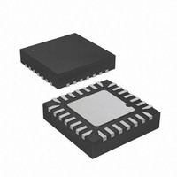
ATMEGA48V-10MMU Atmel, ATMEGA48V-10MMU Datasheet - Page 90

ATMEGA48V-10MMU
Manufacturer Part Number
ATMEGA48V-10MMU
Description
MCU AVR 4K FLASH 10MHZ 28-QFN
Manufacturer
Atmel
Series
AVR® ATmegar
Specifications of ATMEGA48V-10MMU
Core Processor
AVR
Core Size
8-Bit
Speed
10MHz
Connectivity
I²C, SPI, UART/USART
Peripherals
Brown-out Detect/Reset, POR, PWM, WDT
Number Of I /o
23
Program Memory Size
4KB (2K x 16)
Program Memory Type
FLASH
Eeprom Size
256 x 8
Ram Size
512 x 8
Voltage - Supply (vcc/vdd)
1.8 V ~ 5.5 V
Data Converters
A/D 8x10b
Oscillator Type
Internal
Operating Temperature
-40°C ~ 85°C
Package / Case
28-VQFN Exposed Pad, 28-HVQFN, 28-SQFN, 28-DHVQFN
Processor Series
ATMEGA48x
Core
AVR8
Data Bus Width
8 bit
Data Ram Size
512 B
Interface Type
2-Wire, SPI, USART, Serial
Maximum Clock Frequency
10 MHz
Number Of Programmable I/os
23
Number Of Timers
3
Maximum Operating Temperature
+ 85 C
Mounting Style
SMD/SMT
3rd Party Development Tools
EWAVR, EWAVR-BL
Minimum Operating Temperature
- 40 C
On-chip Adc
10 bit, 8 Channel
Package
28MLF EP
Device Core
AVR
Family Name
ATmega
Maximum Speed
10 MHz
Operating Supply Voltage
2.5|3.3|5 V
For Use With
ATSTK600 - DEV KIT FOR AVR/AVR32ATAVRDRAGON - KIT DRAGON 32KB FLASH MEM AVR
Lead Free Status / RoHS Status
Lead free / RoHS Compliant
Available stocks
Company
Part Number
Manufacturer
Quantity
Price
Company:
Part Number:
ATMEGA48V-10MMU
Manufacturer:
ZILOG
Quantity:
1
- Current page: 90 of 378
- Download datasheet (8Mb)
14.3
14.4
90
Timer/Counter Clock Sources
Counter Unit
ATmega48/88/168
The Timer/Counter can be clocked internally, via the prescaler, or by an external clock source on
the T0 pin. The Clock Select logic block controls which clock source and edge the Timer/Counter
uses to increment (or decrement) its value. The Timer/Counter is inactive when no clock source
is selected. The output from the Clock Select logic is referred to as the timer clock (clk
The double buffered Output Compare Registers (OCR0A and OCR0B) are compared with the
Timer/Counter value at all times. The result of the compare can be used by the Waveform Gen-
erator to generate a PWM or variable frequency output on the Output Compare pins (OC0A and
OC0B).
event will also set the Compare Flag (OCF0A or OCF0B) which can be used to generate an Out-
put Compare interrupt request.
The Timer/Counter can be clocked by an internal or an external clock source. The clock source
is selected by the Clock Select logic which is controlled by the Clock Select (CS02:0) bits
located in the Timer/Counter Control Register (TCCR0B). For details on clock sources and pres-
caler, see
The main part of the 8-bit Timer/Counter is the programmable bi-directional counter unit.
14-2
Figure 14-2. Counter Unit Block Diagram
Signal description (internal signals):
Depending of the mode of operation used, the counter is cleared, incremented, or decremented
at each timer clock (clk
selected by the Clock Select bits (CS02:0). When no clock source is selected (CS02:0 = 0) the
timer is stopped. However, the TCNT0 value can be accessed by the CPU, regardless of
whether clk
count operations.
shows a block diagram of the counter and its surroundings.
count
direction
clear
clk
top
bottom
See “Using the Output Compare Unit” on page 117.
Tn
“Timer/Counter0 and Timer/Counter1 Prescalers” on page
T0
is present or not. A CPU write overrides (has priority over) all counter clear or
DATA BUS
TCNTn
T0
). clk
Increment or decrement TCNT0 by 1.
Select between increment and decrement.
Clear TCNT0 (set all bits to zero).
Timer/Counter clock, referred to as clk
Signalize that TCNT0 has reached maximum value.
Signalize that TCNT0 has reached minimum value (zero).
T0
can be generated from an external or internal clock source,
direction
count
clear
bottom
Control Logic
top
TOVn
(Int.Req.)
clk
Tn
for details. The compare match
Clock Select
( From Prescaler )
Detector
Edge
T0
136.
in the following.
2545S–AVR–07/10
Tn
T0
).
Figure
Related parts for ATMEGA48V-10MMU
Image
Part Number
Description
Manufacturer
Datasheet
Request
R

Part Number:
Description:
IC AVR MCU 4K 5V 10MHZ 32-TQFP
Manufacturer:
Atmel
Datasheet:

Part Number:
Description:
IC AVR MCU 4K 10MHZ 1.8V 32-QFN
Manufacturer:
Atmel
Datasheet:

Part Number:
Description:
IC AVR MCU 4K 10MHZ 1.8V 28DIP
Manufacturer:
Atmel
Datasheet:

Part Number:
Description:
IC AVR MCU 4K 5V 10MHZ 32-TQFP
Manufacturer:
Atmel
Datasheet:

Part Number:
Description:
IC AVR MCU 4K 5V 12MHZ 32-QFN
Manufacturer:
Atmel
Datasheet:

Part Number:
Description:
IC AVR MCU 4K 5V 10MHZ 32-QFN
Manufacturer:
Atmel
Datasheet:

Part Number:
Description:
IC AVR MCU 4K 5V 10MHZ 28-DIP
Manufacturer:
Atmel
Datasheet:

Part Number:
Description:
IC AVR MCU 4K 5V 10MHZ 28-DIP
Manufacturer:
Atmel
Datasheet:

Part Number:
Description:
MCU AVR 4KB FLASH 10MHZ 32TQFP
Manufacturer:
Atmel
Datasheet:

Part Number:
Description:
MCU AVR 4KB FLASH 10MHZ 32QFN
Manufacturer:
Atmel
Datasheet:

Part Number:
Description:
MCU AVR 4KB FLASH 20MHZ 28QFN
Manufacturer:
Atmel
Datasheet:


