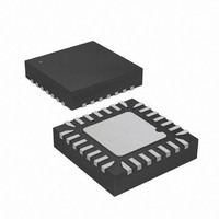
ATMEGA48V-10MMU Atmel, ATMEGA48V-10MMU Datasheet - Page 5

ATMEGA48V-10MMU
Manufacturer Part Number
ATMEGA48V-10MMU
Description
MCU AVR 4K FLASH 10MHZ 28-QFN
Manufacturer
Atmel
Series
AVR® ATmegar
Specifications of ATMEGA48V-10MMU
Core Processor
AVR
Core Size
8-Bit
Speed
10MHz
Connectivity
I²C, SPI, UART/USART
Peripherals
Brown-out Detect/Reset, POR, PWM, WDT
Number Of I /o
23
Program Memory Size
4KB (2K x 16)
Program Memory Type
FLASH
Eeprom Size
256 x 8
Ram Size
512 x 8
Voltage - Supply (vcc/vdd)
1.8 V ~ 5.5 V
Data Converters
A/D 8x10b
Oscillator Type
Internal
Operating Temperature
-40°C ~ 85°C
Package / Case
28-VQFN Exposed Pad, 28-HVQFN, 28-SQFN, 28-DHVQFN
Processor Series
ATMEGA48x
Core
AVR8
Data Bus Width
8 bit
Data Ram Size
512 B
Interface Type
2-Wire, SPI, USART, Serial
Maximum Clock Frequency
10 MHz
Number Of Programmable I/os
23
Number Of Timers
3
Maximum Operating Temperature
+ 85 C
Mounting Style
SMD/SMT
3rd Party Development Tools
EWAVR, EWAVR-BL
Minimum Operating Temperature
- 40 C
On-chip Adc
10 bit, 8 Channel
Package
28MLF EP
Device Core
AVR
Family Name
ATmega
Maximum Speed
10 MHz
Operating Supply Voltage
2.5|3.3|5 V
For Use With
ATSTK600 - DEV KIT FOR AVR/AVR32ATAVRDRAGON - KIT DRAGON 32KB FLASH MEM AVR
Lead Free Status / RoHS Status
Lead free / RoHS Compliant
Available stocks
Company
Part Number
Manufacturer
Quantity
Price
Company:
Part Number:
ATMEGA48V-10MMU
Manufacturer:
ZILOG
Quantity:
1
- Current page: 5 of 378
- Download datasheet (8Mb)
2. Overview
2.1
2545S–AVR–07/10
Block Diagram
The ATmega48/88/168 is a low-power CMOS 8-bit microcontroller based on the AVR enhanced
RISC architecture. By executing powerful instructions in a single clock cycle, the
ATmega48/88/168 achieves throughputs approaching 1 MIPS per MHz allowing the system
designer to optimize power consumption versus processing speed.
Figure 2-1.
The AVR core combines a rich instruction set with 32 general purpose working registers. All the
32 registers are directly connected to the Arithmetic Logic Unit (ALU), allowing two independent
registers to be accessed in one single instruction executed in one clock cycle. The resulting
Block Diagram
Generation
PORT D (8)
Watchdog
Watchdog
Oscillator
Oscillator
8bit T/C 0
8bit T/C 2
USART 0
Circuits /
EEPROM
Timer
Clock
PD[0..7]
POR / BOD &
Supervision
PORT B (8)
16bit T/C 1
Analog
Power
RESET
Comp.
Flash
PB[0..7]
SPI
CPU
debugWIRE
PORT C (7)
A/D Conv.
Bandgap
PROGRAM
Internal
SRAM
PC[0..6]
LOGIC
TWI
ATmega48/88/168
6
ADC[6..7]
2
AVCC
XTAL[1..2]
AREF
GND
RESET
5
Related parts for ATMEGA48V-10MMU
Image
Part Number
Description
Manufacturer
Datasheet
Request
R

Part Number:
Description:
IC AVR MCU 4K 5V 10MHZ 32-TQFP
Manufacturer:
Atmel
Datasheet:

Part Number:
Description:
IC AVR MCU 4K 10MHZ 1.8V 32-QFN
Manufacturer:
Atmel
Datasheet:

Part Number:
Description:
IC AVR MCU 4K 10MHZ 1.8V 28DIP
Manufacturer:
Atmel
Datasheet:

Part Number:
Description:
IC AVR MCU 4K 5V 10MHZ 32-TQFP
Manufacturer:
Atmel
Datasheet:

Part Number:
Description:
IC AVR MCU 4K 5V 12MHZ 32-QFN
Manufacturer:
Atmel
Datasheet:

Part Number:
Description:
IC AVR MCU 4K 5V 10MHZ 32-QFN
Manufacturer:
Atmel
Datasheet:

Part Number:
Description:
IC AVR MCU 4K 5V 10MHZ 28-DIP
Manufacturer:
Atmel
Datasheet:

Part Number:
Description:
IC AVR MCU 4K 5V 10MHZ 28-DIP
Manufacturer:
Atmel
Datasheet:

Part Number:
Description:
MCU AVR 4KB FLASH 10MHZ 32TQFP
Manufacturer:
Atmel
Datasheet:

Part Number:
Description:
MCU AVR 4KB FLASH 10MHZ 32QFN
Manufacturer:
Atmel
Datasheet:

Part Number:
Description:
MCU AVR 4KB FLASH 20MHZ 28QFN
Manufacturer:
Atmel
Datasheet:


