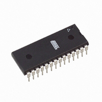
AT89LP828-20PU Atmel, AT89LP828-20PU Datasheet - Page 35

AT89LP828-20PU
Manufacturer Part Number
AT89LP828-20PU
Description
MCU 8051 8K FLASH SPI 28PDIP
Manufacturer
Atmel
Series
89LPr
Datasheet
1.AT89LP428-20AU.pdf
(149 pages)
Specifications of AT89LP828-20PU
Core Processor
8051
Core Size
8-Bit
Speed
20MHz
Connectivity
SPI, UART/USART
Peripherals
Brown-out Detect/Reset, POR, PWM, WDT
Number Of I /o
30
Program Memory Size
8KB (8K x 8)
Program Memory Type
FLASH
Eeprom Size
1K x 8
Ram Size
768 x 8
Voltage - Supply (vcc/vdd)
2.4 V ~ 5.5 V
Oscillator Type
Internal
Operating Temperature
-40°C ~ 85°C
Package / Case
28-DIP (0.300", 7.62mm)
Processor Series
AT89x
Core
8051
Data Bus Width
8 bit
Data Ram Size
768 B
Interface Type
2-Wire, SPI
Maximum Clock Frequency
20 MHz
Number Of Programmable I/os
30
Number Of Timers
3
Maximum Operating Temperature
+ 85 C
Mounting Style
Through Hole
3rd Party Development Tools
PK51, CA51, A51, ULINK2
Development Tools By Supplier
AT89ISP
Minimum Operating Temperature
- 40 C
Lead Free Status / RoHS Status
Lead free / RoHS Compliant
Data Converters
-
Lead Free Status / Rohs Status
Details
Available stocks
Company
Part Number
Manufacturer
Quantity
Price
Company:
Part Number:
AT89LP828-20PU
Manufacturer:
NXP
Quantity:
3 942
10. I/O Ports
10.1
3654A–MICRO–8/09
Port Configuration
The AT89LP428/828 can be configured for between 23 and 30 I/O pins. The exact number of
I/O pins available depends on the package type and the clock and reset options as shown in
Table
Table 10-1.
All port pins on the AT89LP428/828 may be configured to one of four modes: quasi-bidirectional
(standard 8051 port outputs), push-pull output, open-drain output, or input-only. Port modes may
be assigned in software on a pin-by-pin basis as shown in
Table
fuse is enabled, all port pins default to input-only mode after reset. When the fuse is disabled, all
port pins, with the exception of the analog inputs, P2.4, P2.5, P2.6 and P2.7, default to quasi-
bidirectional mode after reset and are weakly pulled high. The analog input pins always reset to
input-only (tristate) mode. Each port pin also has a Schmitt-triggered input for improved input
noise rejection. During Power-down all the Schmitt-triggered inputs are disabled with the excep-
tion of P3.2 (INT0), P3.3 (INT1), P3.6 (RST), P4.0 (XTAL1) and P4.1 (XTAL2) which may be
used to wake up the device. Therefore, P3.2, P3.3, P3.6, P4.0 and P4.1 should not be left float-
ing during Power-down. In addition any pin of Port 1 configured as a GPI input will also remain
active during Power-down to wake-up the device. These interrupt pins should either be disabled
before entering Power-down or they should not be left floating.
Table 10-2.
Clock Source
External Crystal or
Resonator
External Clock
Internal RC Oscillator
PxM0.y
10-1.
10-3. The Tristate-Port User Fuse determines the default state of the port pins. When the
0
0
1
1
I/O Pin Configurations
Configuration Modes for Port x, Bit y
PxM1.y
0
1
0
1
Reset Option
External RST Pin
No external reset
External RST Pin
No external reset
External RST Pin
No external reset
Port Mode
Quasi-bidirectional
Push-pull Output
Input Only (High Impedance)
Open-drain Output
Package
PDIP
TQFP or PLCC
PDIP
TQFP or PLCC
PDIP
TQFP or PLCC
PDIP
TQFP or PLCC
PDIP
TQFP or PLCC
PDIP
TQFP or PLCC
Table 10-2
AT89LP428/828
using the registers listed in
Number of I/O Pins
23
27
24
28
24
28
25
29
25
29
26
30
35


