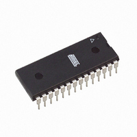
AT89LP828-20PU Atmel, AT89LP828-20PU Datasheet - Page 48

AT89LP828-20PU
Manufacturer Part Number
AT89LP828-20PU
Description
MCU 8051 8K FLASH SPI 28PDIP
Manufacturer
Atmel
Series
89LPr
Datasheet
1.AT89LP428-20AU.pdf
(149 pages)
Specifications of AT89LP828-20PU
Core Processor
8051
Core Size
8-Bit
Speed
20MHz
Connectivity
SPI, UART/USART
Peripherals
Brown-out Detect/Reset, POR, PWM, WDT
Number Of I /o
30
Program Memory Size
8KB (8K x 8)
Program Memory Type
FLASH
Eeprom Size
1K x 8
Ram Size
768 x 8
Voltage - Supply (vcc/vdd)
2.4 V ~ 5.5 V
Oscillator Type
Internal
Operating Temperature
-40°C ~ 85°C
Package / Case
28-DIP (0.300", 7.62mm)
Processor Series
AT89x
Core
8051
Data Bus Width
8 bit
Data Ram Size
768 B
Interface Type
2-Wire, SPI
Maximum Clock Frequency
20 MHz
Number Of Programmable I/os
30
Number Of Timers
3
Maximum Operating Temperature
+ 85 C
Mounting Style
Through Hole
3rd Party Development Tools
PK51, CA51, A51, ULINK2
Development Tools By Supplier
AT89ISP
Minimum Operating Temperature
- 40 C
Lead Free Status / RoHS Status
Lead free / RoHS Compliant
Data Converters
-
Lead Free Status / Rohs Status
Details
Available stocks
Company
Part Number
Manufacturer
Quantity
Price
Company:
Part Number:
AT89LP828-20PU
Manufacturer:
NXP
Quantity:
3 942
11.5.1
11.5.2
48
AT89LP428/828
Mode 0 – 8-bit PWM with 8-bit Logarithmic Prescaler
Mode 1 – 8-bit PWM with 8-bit Linear Prescaler
In Mode 0, TLx acts as a logarithmic prescaler driving 8-bit counter THx (see
PSCx bits in TCONB control the prescaler value. On THx overflow, the duty cycle value in RHx
is transferred to OCRx and the output pin is set high. When the count in THx matches OCRx, the
output pin is cleared low. The following formulas give the output frequency and duty cycle for
Timer 0 in PWM mode 0. Timer 1 in PWM mode 0 is identical to Timer 0.
Figure 11-6. Timer/Counter 1 PWM Mode 0
In Mode 1, TLx provides linear prescaling with an 8-bit auto-reload from RLx (see
page
THx overflow, the duty cycle value in RHx is transferred to OCRx and the output pin is set high.
When the count in THx matches OCRx, the output pin is cleared low. The following formulas
give the output frequency and duty cycle for Timer 0 in PWM mode 1. Timer 1 in PWM mode 1 is
identical to Timer 0.
INT1 Pin
49). On TLx overflow, TLx is loaded with the value of RLx. THx acts as an 8-bit counter. On
GATE
OSC
TR1
Mode 0:
Mode 1:
÷TPS
Control
f
f
OUT
OUT
=
=
Duty Cycle %
Duty Cycle %
Oscillator Frequency
------------------------------------------------------ -
Oscillator Frequency
------------------------------------------------------ -
PSC1
256
256
×
(8 Bits)
×
(
TL1
256 RL0
2
PSC0
=
=
–
100
100
+
1
(8 Bits)
(8 Bits)
OCR1
)
RH1
TH1
×
×
×
RH0
----------- -
×
RH0
----------- -
256
256
-------------------- -
TPS
-------------------- -
TPS
=
1
1
+
+
1
1
Figure
3654A–MICRO–8/09
Figure 11-7 on
11-6). The
T1


