AT89LP828-20PU Atmel, AT89LP828-20PU Datasheet - Page 82

AT89LP828-20PU
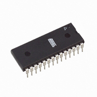
Manufacturer Part Number
AT89LP828-20PU
Description
MCU 8051 8K FLASH SPI 28PDIP
Manufacturer
Atmel
Series
89LPr
Datasheet
1.AT89LP428-20AU.pdf
(149 pages)
Specifications of AT89LP828-20PU
Core Processor
8051
Core Size
8-Bit
Speed
20MHz
Connectivity
SPI, UART/USART
Peripherals
Brown-out Detect/Reset, POR, PWM, WDT
Number Of I /o
30
Program Memory Size
8KB (8K x 8)
Program Memory Type
FLASH
Eeprom Size
1K x 8
Ram Size
768 x 8
Voltage - Supply (vcc/vdd)
2.4 V ~ 5.5 V
Oscillator Type
Internal
Operating Temperature
-40°C ~ 85°C
Package / Case
28-DIP (0.300", 7.62mm)
Processor Series
AT89x
Core
8051
Data Bus Width
8 bit
Data Ram Size
768 B
Interface Type
2-Wire, SPI
Maximum Clock Frequency
20 MHz
Number Of Programmable I/os
30
Number Of Timers
3
Maximum Operating Temperature
+ 85 C
Mounting Style
Through Hole
3rd Party Development Tools
PK51, CA51, A51, ULINK2
Development Tools By Supplier
AT89ISP
Minimum Operating Temperature
- 40 C
Lead Free Status / RoHS Status
Lead free / RoHS Compliant
Data Converters
-
Lead Free Status / Rohs Status
Details
Available stocks
Company
Part Number
Manufacturer
Quantity
Price
Company:
Part Number:
AT89LP828-20PU
Manufacturer:
NXP
Quantity:
3 942
82
AT89LP428/828
Reception is initiated by the condition REN = 1 and R1 = 0. At the next clock cycle, the RX Con-
trol unit writes the bits 11111110 to the receive shift register and activates RECEIVE in the next
clock phase. RECEIVE enables Shift Clock to alternate output function line of P3.1. As data bits
come in from the right, “1”s shift out to the left. When the “0” that was initially loaded into the
right-most position arrives at the left-most position in the shift register, it flags the RX Control
block to do one last shift and load SBUF. Then RECEIVE is cleared and RI is set.
The relationship between the shift clock and data is determined by the combination of the SM2
and SMOD1 bits as listed in
idle state of the clock when not currently transmitting/receiving. The SMOD1 bit determines if the
output data is stable for both edges of the clock, or just one.
Table 16-5.
SM2
0
0
1
1
SMOD1
Mode 0 Clock and Data Modes
0
1
0
1
Clock Idle
High
High
Low
Low
Table 16-5
and shown in
Negative edge of clock
Negative edge of clock
While clock is high
While clock is low
Data Changed
Figure
16-2. The SM2 bit determines the
Negative edge of clock
Positive edge of clock
Positive edge of clock
Positive edge of clock
Data Sampled
3654A–MICRO–8/09


