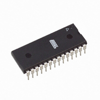
AT89LP828-20PU Atmel, AT89LP828-20PU Datasheet - Page 61

AT89LP828-20PU
Manufacturer Part Number
AT89LP828-20PU
Description
MCU 8051 8K FLASH SPI 28PDIP
Manufacturer
Atmel
Series
89LPr
Datasheet
1.AT89LP428-20AU.pdf
(149 pages)
Specifications of AT89LP828-20PU
Core Processor
8051
Core Size
8-Bit
Speed
20MHz
Connectivity
SPI, UART/USART
Peripherals
Brown-out Detect/Reset, POR, PWM, WDT
Number Of I /o
30
Program Memory Size
8KB (8K x 8)
Program Memory Type
FLASH
Eeprom Size
1K x 8
Ram Size
768 x 8
Voltage - Supply (vcc/vdd)
2.4 V ~ 5.5 V
Oscillator Type
Internal
Operating Temperature
-40°C ~ 85°C
Package / Case
28-DIP (0.300", 7.62mm)
Processor Series
AT89x
Core
8051
Data Bus Width
8 bit
Data Ram Size
768 B
Interface Type
2-Wire, SPI
Maximum Clock Frequency
20 MHz
Number Of Programmable I/os
30
Number Of Timers
3
Maximum Operating Temperature
+ 85 C
Mounting Style
Through Hole
3rd Party Development Tools
PK51, CA51, A51, ULINK2
Development Tools By Supplier
AT89ISP
Minimum Operating Temperature
- 40 C
Lead Free Status / RoHS Status
Lead free / RoHS Compliant
Data Converters
-
Lead Free Status / Rohs Status
Details
Available stocks
Company
Part Number
Manufacturer
Quantity
Price
Company:
Part Number:
AT89LP828-20PU
Manufacturer:
NXP
Quantity:
3 942
13. Compare/Capture Array
3654A–MICRO–8/09
Figure 12-8. Timer 2 in Clock-out Mode
The AT89LP428/828 includes a four channel Compare/Capture Array (CCA) that performs a
variety of timing operations including input event capture, output compare waveform generation
and pulse width modulation (PWM). Timer 2 serves as the time base for the four 16-bit com-
pare/capture modules. The CCA has the following features:
The block diagram of the CCA is given in
register and a 16-bit data register. The channel registers are not directly accessible. The CCA
address register T2CCA provides an index into the array. The control, data low and data high
bytes of the currently indexed channel are accessed through the T2CCC, T2CCL and T2CCH
registers, respectively.
Each channel can be individually configured for capture or compare mode. Capture mode is the
default setting. During capture mode, the current value of the time base is copied into the chan-
nel’s data register when the specified external or internal event occurs. An interrupt flag is set at
the same time and the time base may be optionally cleared. To enable compare mode, the
CCMx bit in the channel’s control register (CCCx) should be set to 1. In compare mode an inter-
rupt flag is set and an output pin is optionally toggled when the value of the time base matches
the value of the channel’s data register. The time base may also be optionally cleared on a com-
pare match.
• Four 16-bit Compare/Capture channels
• Common time base provided by Timer 2
• Selectable external and internal capture events including pin change, timer overflow and
• Symmetric/Asymmetric PWM with selectable polarity
• Multi-phasic PWM outputs
• One interrupt flag per channel with a common interrupt vector
comparator output change
T2EX PIN
T2 PIN
OSC
÷TPS
Transition
Detector
Figure
C/T2
EXEN2
TR2
13-1. Each channel consists of an 8-bit control
RCAP2L
TL2
÷2
EXF2
AT89LP428/828
RCAP2H
TH2
Interrupt
T2OE
Timer 2
61


