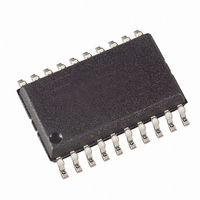
ATTINY861-20SU Atmel, ATTINY861-20SU Datasheet - Page 117

ATTINY861-20SU
Manufacturer Part Number
ATTINY861-20SU
Description
IC MCU AVR 8K FLASH 20MHZ 20SOIC
Manufacturer
Atmel
Series
AVR® ATtinyr
Datasheet
1.ATAVRMC321.pdf
(242 pages)
Specifications of ATTINY861-20SU
Core Processor
AVR
Core Size
8-Bit
Speed
20MHz
Connectivity
USI
Peripherals
Brown-out Detect/Reset, POR, PWM, WDT
Number Of I /o
16
Program Memory Size
8KB (4K x 16)
Program Memory Type
FLASH
Eeprom Size
512 x 8
Ram Size
512 x 8
Voltage - Supply (vcc/vdd)
2.7 V ~ 5.5 V
Data Converters
A/D 11x10b
Oscillator Type
Internal
Operating Temperature
-40°C ~ 85°C
Package / Case
20-SOIC (7.5mm Width)
Cpu Family
ATtiny
Device Core
AVR
Device Core Size
8b
Frequency (max)
20MHz
Interface Type
USI
Total Internal Ram Size
512Byte
# I/os (max)
16
Number Of Timers - General Purpose
2
Operating Supply Voltage (typ)
3.3/5V
Operating Supply Voltage (max)
5.5V
Operating Supply Voltage (min)
2.7V
On-chip Adc
11-chx10-bit
Instruction Set Architecture
RISC
Operating Temp Range
-40C to 85C
Operating Temperature Classification
Industrial
Mounting
Surface Mount
Pin Count
20
Package Type
SOIC
Processor Series
ATTINY8x
Core
AVR8
Data Bus Width
8 bit
Data Ram Size
512 B
Maximum Clock Frequency
20 MHz
Number Of Programmable I/os
16
Number Of Timers
2
Operating Supply Voltage
2.7 V to 5.5 V
Maximum Operating Temperature
+ 85 C
Mounting Style
SMD/SMT
3rd Party Development Tools
EWAVR, EWAVR-BL
Development Tools By Supplier
ATAVRDRAGON, ATSTK500, ATSTK600, ATAVRISP2, ATAVRONEKIT, ATAVRMC320
Minimum Operating Temperature
- 40 C
For Use With
ATSTK600 - DEV KIT FOR AVR/AVR32ATAVRBC100 - REF DESIGN KIT BATTERY CHARGER770-1007 - ISP 4PORT ATMEL AVR MCU SPI/JTAG770-1004 - ISP 4PORT FOR ATMEL AVR MCU SPI
Lead Free Status / RoHS Status
Lead free / RoHS Compliant
Available stocks
Company
Part Number
Manufacturer
Quantity
Price
12.12.3
2588E–AVR–08/10
TCCR1C – Timer/Counter1 Control Register C
• Bits 7,6 – COM1A1S, COM1A0S: Comparator A Output Mode, Shadow Bits 1 and 0
These are shadow bits of COM1A1 and COM1A0 in TCCR1A. Writing to bits COM1A1S and
COM1A0S will also change bits COM1A1 and COM1A0 in TCCR1A. Similary, changes written
to bits COM1A1 and COM1A0 in TCCR1A will show here.
See
• Bits 5,4 – COM1B1S, COM1B0S: Comparator B Output Mode, Shadow Bits 1 and 0
These are shadow bits of COM1B1 and COM1B0 in TCCR1A. Writing to bits COM1B1S and
COM1B0S will also change bits COM1B1 and COM1B0 in TCCR1A. Similary, changes written
to bits COM1B1 and COM1B0 in TCCR1A will show here.
See
• Bits 3,2 – COM1D1, COM1D0: Comparator D Output Mode, Bits 1 and 0
These bits control the behaviour of the Waveform Output (OCW1D) and the connection of the
Output Compare pin (OC1D). If one or both of the COM1D1:0 bits are set, the OC1D output
overrides the normal port functionality of the I/O pin it is connected to. The complementary
OC1D output is connected only in PWM modes when the COM1D1:0 bits are set to “01”. Note
that the Data Direction Register (DDR) bit corresponding to the OC1D pin must be set in order to
enable the output driver.
The function of the COM1D1:0 bits depends on the PWM1D and WGM11:10 bit settings.
12-18
PWM).
Table 12-18. Compare Output Mode, Normal Mode (non-PWM)
Table 12-19
set to Fast PWM Mode.
Table 12-19. Compare Output Mode, Fast PWM Mode
Bit
0x27 (0x47)
Read/Write
Initial value
COM1D1:0
COM1D1:0
“TCCR1A – Timer/Counter1 Control Register A” on page 112
“TCCR1A – Timer/Counter1 Control Register A” on page 112
00
01
10
11
00
01
10
11
shows the COM1D1:0 bit functionality when the PWM1D bit is set to a Normal Mode (non-
shows the COM1D1:0 bit functionality when the PWM1D and WGM11:10 bits are
COM1A1
OCW1D Behaviour
Normal port operation.
Cleared on Compare Match. Set when TCNT1=0x000.
Cleared on Compare Match. Set when TCNT1=0x000.
Set on Compare Match. Cleared when TCNT1=0x000.
R/W
OCW1D Behaviour
Normal port operation.
Toggle on Compare Match.
Clear on Compare Match.
Set on Compare Match.
S
7
0
COM1A0
R/W
S
6
0
COM1B1
R/W
S
5
0
COM1B0
R/W
S
4
0
COM1D1
R/W
3
0
COM1D0
R/W
2
0
OC1D Pin
Disconnected
Connected
Connected
Connected
OC1D Pin
Disconnected
Connected
Connected
Connected
for information on bit usage.
for information on bit usage.
FOC1D
R/W
1
0
PWM1D
R/W
OC1D Pin
Disconnected
Disconnected
Disconnected
Disconnected
0
0
Disconnected
Disconnected
OC1D Pin
Disconnected
Connected
TCCR1C
Table
117


