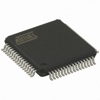
AT90CAN64-16AUR Atmel, AT90CAN64-16AUR Datasheet - Page 175

AT90CAN64-16AUR
Manufacturer Part Number
AT90CAN64-16AUR
Description
MCU AVR 64K FLASH 16MHZ 64TQFP
Manufacturer
Atmel
Series
AVR® 90CANr
Datasheet
1.AT90CAN32-16AUR.pdf
(428 pages)
Specifications of AT90CAN64-16AUR
Core Processor
AVR
Core Size
8-Bit
Speed
16MHz
Connectivity
CAN, EBI/EMI, I²C, SPI, UART/USART
Peripherals
Brown-out Detect/Reset, POR, PWM, WDT
Number Of I /o
53
Program Memory Size
64KB (64K x 8)
Program Memory Type
FLASH
Eeprom Size
2K x 8
Ram Size
4K x 8
Voltage - Supply (vcc/vdd)
2.7 V ~ 5.5 V
Data Converters
A/D 8x10b
Oscillator Type
Internal
Operating Temperature
-40°C ~ 85°C
Package / Case
64-TQFP, 64-VQFP
Data Bus Width
8 bit
Data Ram Size
4 KB
Mounting Style
SMD/SMT
Lead Free Status / RoHS Status
Lead free / RoHS Compliant
Available stocks
Company
Part Number
Manufacturer
Quantity
Price
- Current page: 175 of 428
- Download datasheet (6Mb)
16.2.4
16.2.5
16.3
7679H–CAN–08/08
Data Modes
SPI Status Register – SPSR
SPI Data Register – SPDR
• Bit 7 – SPIF: SPI Interrupt Flag
When a serial transfer is complete, the SPIF flag is set. An interrupt is generated if SPIE in
SPCR is set and global interrupts are enabled. If SS is an input and is driven low when the SPI is
in Master mode, this will also set the SPIF flag. SPIF is cleared by hardware when executing the
corresponding interrupt handling vector. Alternatively, the SPIF bit is cleared by first reading the
SPI Status Register with SPIF set, then accessing the SPI Data Register (SPDR).
• Bit 6 – WCOL: Write COLlision Flag
The WCOL bit is set if the SPI Data Register (SPDR) is written during a data transfer. The
WCOL bit (and the SPIF bit) are cleared by first reading the SPI Status Register with WCOL set,
and then accessing the SPI Data Register.
• Bit 5..1 – Res: Reserved Bits
These bits are reserved bits in the AT90CAN32/64/128 and will always read as zero.
• Bit 0 – SPI2X: Double SPI Speed Bit
When this bit is written logic one the SPI speed (SCK Frequency) will be doubled when the SPI
is in Master mode (see
clock periods. When the SPI is configured as Slave, the SPI is only guaranteed to work at f
or lower.
The SPI interface on the AT90CAN32/64/128 is also used for program memory and EEPROM
downloading or uploading. See
gramming and verification.
• Bits 7:0 - SPD7:0: SPI Data
The SPI Data Register is a read/write register used for data transfer between the Register File
and the SPI Shift Register. Writing to the register initiates data transmission. Reading the regis-
ter causes the Shift Register Receive buffer to be read.
There are four combinations of SCK phase and polarity with respect to serial data, which are
determined by control bits CPHA and CPOL. The SPI data transfer formats are shown in
16-3
Bit
Read/Write
Initial Value
Bit
Read/Write
Initial Value
and
Figure
SPD7
SPIF
R/W
R
X
7
0
7
16-4. Data bits are shifted out and latched in on opposite edges of the SCK sig-
WCOL
SPD6
R/W
Table
R
X
6
0
6
16-4). This means that the minimum SCK period will be two CPU
SPD5
R/W
“SPI Serial Programming Overview” on page 348
R
5
–
0
5
X
SPD4
R/W
4
–
R
0
4
X
SPD3
R/W
R
X
3
–
0
3
SPD2
R/W
R
X
2
–
0
2
AT90CAN32/64/128
SPD1
R/W
R
1
–
0
1
X
SPI2X
SPD0
R/W
R/W
0
0
0
X
Undefined
SPSR
SPDR
for serial pro-
Figure
clkio
175
/4
Related parts for AT90CAN64-16AUR
Image
Part Number
Description
Manufacturer
Datasheet
Request
R

Part Number:
Description:
Manufacturer:
Atmel Corporation
Datasheet:

Part Number:
Description:
Manufacturer:
Atmel Corporation
Datasheet:

Part Number:
Description:
IC MCU AVR 64K FLASH 64-TQFP
Manufacturer:
Atmel
Datasheet:

Part Number:
Description:
IC MCU AVR 64K FLASH 64-QFN
Manufacturer:
Atmel
Datasheet:

Part Number:
Description:
At90can128 8-bit Avr Microcontroller With 32k Bytes Of Isp Flash And Can Controller
Manufacturer:
ATMEL Corporation
Datasheet:

Part Number:
Description:
8-bit Microcontrollers - MCU 64 KB FLASH - 16MHz
Manufacturer:
Atmel

Part Number:
Description:
8-bit Microcontrollers - MCU Microcontroller
Manufacturer:
Atmel

Part Number:
Description:
DEV KIT FOR AVR/AVR32
Manufacturer:
Atmel
Datasheet:


